 Facebook
 Google
 GitHub
 Linkedin
Use LTspice to Understand the LM741 OpAmp
An inside look at how the 741 operational amplifier operates with LTspice simulation. We'll go over internal structure and differential amplifiers and continue with everything you've ever needed to know about this operational amplifier.
The 741 op-amp shares with most op-amps an internal structure consisting of three gain stages:
- Differential amplifier — provides high differential amplification (gain), with rejection of common-mode signal, low noise, high input impedance, and drives a
- Voltage amplifier — provides high voltage gain, a single pole frequency rolloff, and in turn drives the
- Output amplifier — provides high current gain (low output impedance), along with output current limiting, and output short-circuit protection.
It's that easy!
Well, not really.
Assuming you've downloaded LTspice, open up the LM741 Model in LTspiceIV\examples\Educational directory of your LTspice
In part 1 we will mainly be focusing on the input stage and the differential amplifier. Part 2 will consist of the voltage amplifier and output amplifier.
Before reading further you should be comfortable with the following equations that rule transistors:
$$I_{C} = \beta I_{B}$$
$$I_{E} = \frac{ (1+\beta)}{I_{B}}$$
What the Heck is a Differential Amplifier?
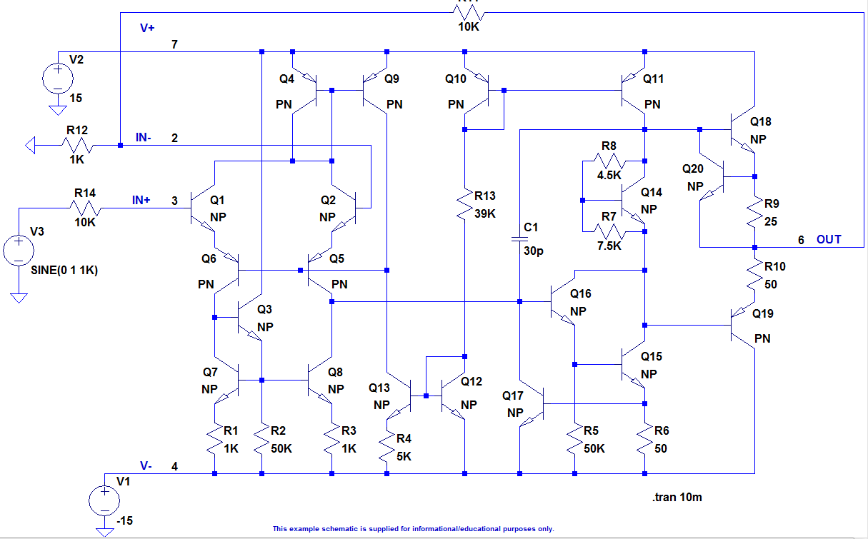
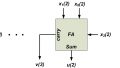
Figure 1 (Click to enlarge)
Current Mirrors
Well, before we get into a differential amplifier we must understand the analog building block called a current mirror. A current mirror is a circuit of the configuration in Figure 1. Start with a current $$I_{ref}$$ which flows into the transistor Q1 in the figure below. A transistor with its collector tied to its base is called a “diode connected transistor” this creates an ideal diode. In turn, this produces a voltage drop across the transistor Q1 of $$V_{be}$$ (about 0.7 volts). Now, since the base and emitter of Q2 is identical and the base-emitter voltage of the transistor Q2 equals the transistor Q1, the same current that flows through Q1, flows through Q2...Well...roughly the same. As you can see the $$I_{mirror}$$ is a factor of
$$\frac{\beta}{\beta + 2}$$
This works out to be roughly 98% of the current of Q1.
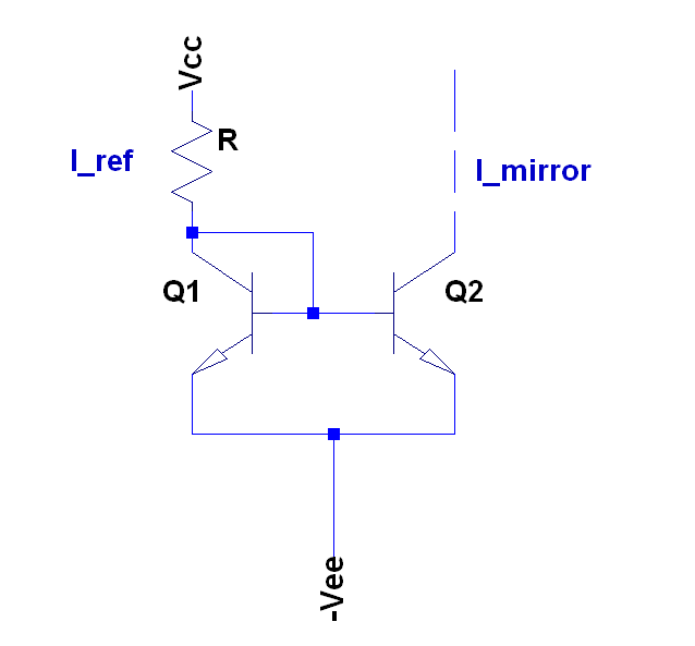
Figure 2
To derive the equation for $$I_{mirror}$$:
$$I_{ref} =I_{B} + I_{C}$$ (Q1)
$$I_{ref} = I_{B} + \frac{\beta I_{B}}{2}$$
$$I_{ref} = \frac{I_{B}(2+\beta)}{2}$$
Therefore,
$$I_{B} = \frac{2I_{ref}}{2 + \beta}$$
$$I_{mirror} = \frac{\beta I_{B}}{2}$$
$$I_{mirror} = \frac{2 \beta I_{ref}}{2(2+\beta)}$$
$$I_{mirror} = \frac{\beta I_{ref}}{\beta + 2}$$
Differential Amplifiers
Let me confuse you first and overstate the simplicity of its operation by saying that, simply put, a differential amplifier is a type of amplifier that only amplifies the difference between two voltages and nothing more (idealistically). Besides using different variations of the word "amplify" and simplifying way too many times in that last sentence, its operation is a little more complex than I’ve led you to believe thus far. Let's get into the detail.
Figure 3 Long-Tailed Pair
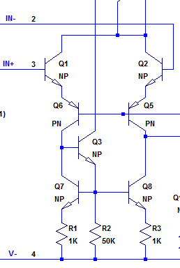
This is a differential amplifier, often referred to as a long-tailed pair. You can see this fundamental analog building block configuration being made between Q4, Q9, Q1, and Q2 of the schematic of the LM741 above. The 741 has some additional components involved with its differential pair input, but we will get into that later. Q4 and Q9 make the current mirror of the PNP variety. Check your understanding by working out the math much like we did for the NPN, taking note of the sign differentiation of a PNP (I'll leave this as an exercise for you).
When the voltage at both inputs is equal, then the current $$I_{e}$$ is split equally between the two transistors Q1 and Q2. The purpose of $$I_{e}$$ is to allocate a set amount of current to the two transistors such that when there is a difference at the inputs we get a differential amplifier. That is, when we increase the voltage at the non-inverting input relative to the inverting input Q2 gets more of the current than Q1, and vice versa. I think this will be made clearer after a study of the simulation below.
Differential Amplifier Simulation
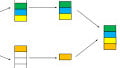
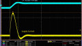
Attach the two voltage sources to your simulation as follows, take out the feedback and change both input resistors to 1k as such:
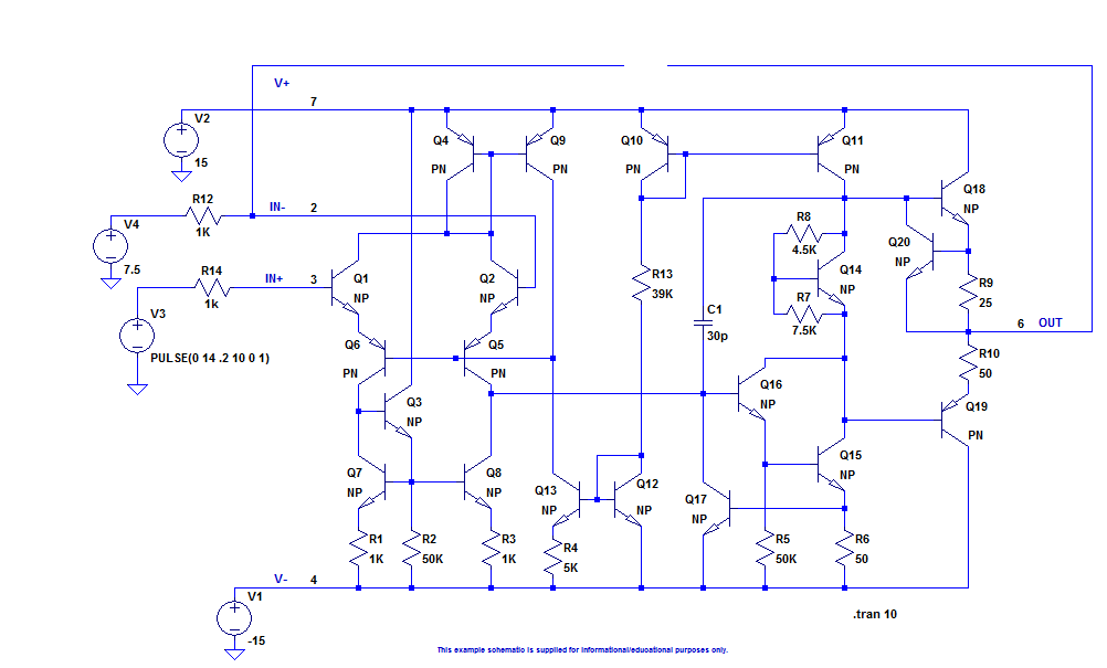
Figure 4
And Generate the following output:
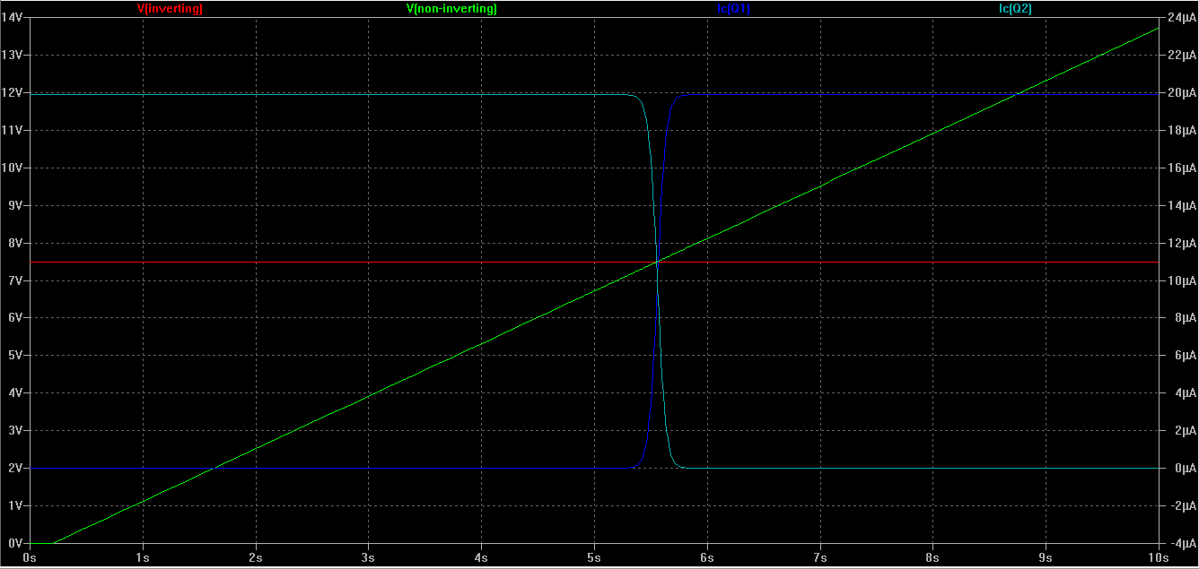
Figure 5
As the non-inverting input reaches the inverting inputs voltage the current in Q1 and Q2 is equal. Also note how the current in each differs depending on the difference in voltage between the two inputs.
In the 741 the current $$I_{e}$$ of the long-tailed pair in figure 3 above is actually produced by the additional circuitry in the input stage. The input stage is made up of Q1, Q2, Q3, Q5, Q6, Q7, and Q8.
Q12, Q13 , and R13 are important to the input stage as well because they create the reference current. The bias for the input stage is created with Q12, Q13 and R4 and current mirror Q4, Q9.
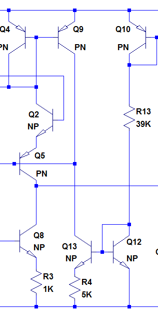
$$I_{ref}$$ can be calculated as follows:
$$I_{ref} = \frac{V_{+} - V_{EBQ10} - V_{BEQ12} - (-V_{-})}{R_{13}}$$ where, $$I_{ref}$$ is the current flowing through the right side of the circuit (Q10, R13, Q12)
Q12, Q13 and R4 create a Widlar current source. The first step to understanding a Widlar current source is to do some research on the pioneer and analog legend Bob Widlar, an eccentric personality of the analog world, and inventor of the Widlar current mirror among many other things. He, along with others I will mention, make up the original analog gods. It’s VERY important to read about them.
Anyway, I digress... A Widlar Current source differs from a normal current source because a resistor is added to the emitter of the output stage transistor. In the 741's schematic this is resistor R4.This is more so a practice in saving IC space when designing the chips. Instead of using large resistors to create small currrents, the Widlar current source creates small currents with small resistors. To calculate the current $$I_C$$ (of Q13) , which is the “output” of the Widlar current source follow the KVL around the base emitter loop of this section of the circuit:
$$V_{BEQ12} = V_{BEQ13} + I_{EQ13} R_{4} = V_{BEQ13} + (\beta + 1) I_{BQ13} R_{4}$$
Where, $$I_{IN} = I_{CQ12}, I_{OUT} = I_{CQ13}$$
For a BJT, $$V_{BE} = V_{T} \ln (\frac{I_{C}}{I_{S}}) so, $$
$$V_{T} \ln (\frac{I_{IN}}{I_{S1}}) = V_{T} \ln (\frac{I_{OUT}}{I_{S2}}) + I_{OUT} R_{4}$$
$$I_{OUT} R_{4} = V_{T} \ln (\frac{I_{IN}}{I_{OUT}}) $$
From here you can solve iteratively.
That wraps up the input stage! Stay tuned for part 2!
Next Article in Series: Use LTspice to Understand the LM741 OpAmp: Part 2
Related Content


Hello! That’s a very interesting article and I am looking forward to read the next chapter to understand what the rest of the transistors are doing.
Also, thanks for the link to the interview, that was very interesting to read!
Very nice article !
Just a small typo in the first equations of transistors, should be multiplication, not division like shown.