 Facebook
 Google
 GitHub
 Linkedin
The JTAG Test Access Port (TAP) State Machine
In this article, we’re going to look at the test access state machine in detail and even see some pseudocode for a simple JTAG interface.
In the first part to this series, we looked at JTAG, the ubiquitous microcontroller/FPGA/ASIC interface standard. But while we covered a lot of ground regarding instructions and registers, we still need to understand how to operate the JTAG test access port (TAP).
As mentioned in the previous article, the TAP is controlled through a state machine, which has two paths depending on whether we are loading an instruction, or reading/writing a data register. In this part, we’re going to look at the state machine in detail, and we’ll even see some pseudocode for a simple JTAG interface.
The TAP State Machine
The state machine is shown, as it appears in the IEEE 1149.1-2013 standard, in Figure 1 below.
The state machine is simple, comprising two paths:
- The data register (DR) path (shown in green), used for loading instructions
- The instruction register (IR) path (shown in blue), used for reading/writing data from/to data registers, including the boundary scan register (BSR)
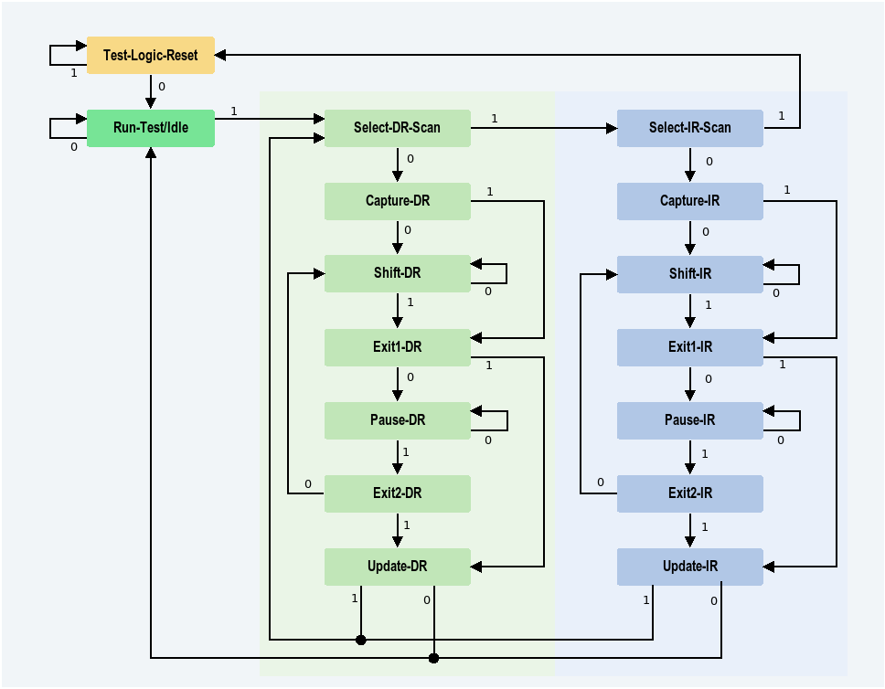
Figure 1. TAP state machine, as shown in the IEEE 1149.1-2013 standard. Click here for a larger version.
The state machine progresses on the test clock (TCK) edge, with the value of the test mode select (TMS) pin controlling the behavior.
Assuming the state machine begins at Test-Logic-Reset, we begin by clocking a TMS = 0 to enter the Run-Test/Idle state, then clock a TMS = 1 to begin selecting a path.
The roles of the different states are summarized briefly in Figure 2.
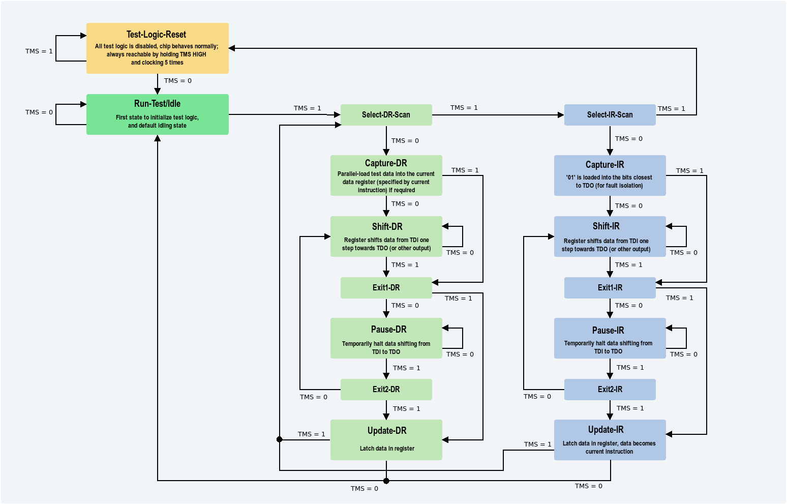
Figure 2. TAP state machine with state descriptions. Click here for a larger version.
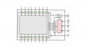
To aid in understanding these states, look again at the JTAG system from the previous article, Figure 3.

Figure 3. JTAG architecture
The TAP controller manages the state machine, and depending on the state selected, the output MUX is switched.
The two paths are:
- The instruction capture-shift path
- The data capture-shift path
Note how the boundary-scan register, which comprises the boundary-scan cells around the IO pins, is one of the data registers. Data registers are shift-registers, and can be of arbitrary length.
Capture, Update, and Shift States
The most ‘active’ states are the capture, shift, and update states.
The capture state is perhaps the most mysterious, performing different actions for the data path compared to the instruction path. Here, capture means parallel loading data into a shift register, as opposed to shifting the data in serial into the register. Shift means, as one might expect, shifting data into the shift register. Then, the update stage latches the register, and the state machine can reset.
Specifically, Capture-DR is the state where, if needed, test data can be parallel-loaded into the shift-capture path of the current data register. (The current data register is set by the current instruction which was previously set.) This means that data is loaded, in parallel, into the data register selected by the current instruction, as opposed to shifting in.
Capture-IR is used for fault isolation in the JTAG system, though the standard is vague about its purpose. A fixed logic value (which must end in {...01}) is loaded in parallel into the instruction register shift-capture path. This is to say, the instruction register is parallel-loaded (instead of shifting) with a fixed logic value.
The Shift-DR and Shift-IR states are the main states for serial-loading data into either data registers or the instruction register. While the state machine is in one of these states, TMS is held LOW, until the shifting operation is complete. The Update-DR and Update-IR states latch the data into the registers, setting the data in the instruction register as the current instruction (and in doing so, setting the current data register for the next cycle).
Examples of manipulating the TAP state machine are often given in the form of timing diagrams, but such diagrams are limited in their ability to convey information, so the interested reader is referred to the JTAG standard itself for further information, including implementation suggestions for various logic blocks.
JTAG Interface Pseudocode
To flesh out the ideas above, in this section we will assemble some pseudocode that might control a JTAG interface (which can be as simple as a microcontroller development board). The code implements the most basic functions without any error checking or special handling of instructions. A few delays are included to manage timing, including a short delay to accommodate systems with multi-tasking that cannot guarantee timing.
// Define pins
JTAG_TMS = PA01
JTAG_TCK = PA02
JTAG_TDI = PA03
JTAG_TDO = PA04
// Create a string of five 1’s, for forcing reset
tms_reset_str = {1,1,1,1,1}
// JTAG FUNCTIONS
// Transmit a constant string to the TAP, without setting TDI or TDO
transmit_tms_str(tms_str)
{
for i = 0 : len(tms_str)
{
set_pin(JTAG_TMS, tms_str[i])
jtag_short_delay()
set_pin(JTAG_TCK, HIGH)
jtag_clock_delay()
set_pin(JTAG_TCK,LOW)
jtag_clock_delay()
}
}
shift_tdi_str(tdi_str)
{
    set_pin(JTAG_TMS, LOW) // Hold TMS LOW while shifting<br />
<br />
for i = 0 : len(tdi_str)
{
set_pin(JTAG_TDI,tdi_str[i])
jtag_short_delay()
set_pin(JTAG_TCK, HIGH)
jtag_clock_delay()
set_pin(JTAG_TCK, LOW)
jtag_clock_delay()
}
}
shift_tdo_str(length)
{
// This function returns the string shifted out from TDO
set_pin(JTAG_TMS, LOW) // Hold TMS LOW while shifting
    output_str = {}<br />
<br />
for i = 0 : length
{
set_pin(JTAG_TCK, HIGH)
jtag_short_delay()
output_str += read_pin(JTAG_TDO)
jtag_clock_delay()
set_pin(JTAG_TCK, LOW)
jtag_clock_delay()
}
return output_str
}
reset_jtag()
{
transmit_tms_str(tms_reset_str)
}
load_jtag_instruction(instr)
{
// Assuming we're in run-test/idle
// Note: No error checking, early exiting, or pausing is
// implemented here
transmit_tms_str( {1,1,0,0} ) // Puts us at Shift-IR state
shift_tdi_str( instr ) // Shift in the instruction data
transmit_tms_str( {1,0,1,1,0} ) // Return to Run-Test/Idle
}
read_jtag_register(reg_length)
{
// This function reads the current data register (set by most
// recent instruction)
// Assuming we're in run-test/idle
// Note: No error checking, early exiting, or pausing is
// implemented here
transmit_tms_str( {1,0,0} ) // Puts us at Shift-DR state
reg_str = shift_tdo_str(reg_length) // Shift out register data
transmit_tms_str( {1,0,1,1,0} ) // Return to Run-Test/Idle
return reg_str
}
You can see a practical example of JTAG interface programming if you browse the Black Magic Probe source, available on Github here. (In particular, look at the src/platforms/ directory and the src/include/ directory).
Conclusion
We have now seen the most important part of the JTAG TAP, its state machine. The material covered in the first two parts of this series can be found in the IEEE 1149.1-2013 standard, along with many helpful implementation hints and details.
From here, we will be getting more practical, looking at various JTAG interfaces available, talking about pinouts and connectors often used, and finally taking a closer look at the Arm Debug Interface (ADI) for an example of JTAG in practice.
Related Content


The following is backwards:
The data register (DR) path (shown in green), used for loading instructions
The instruction register (IR) path (shown in blue), used for reading/writing data from/to data