 Facebook
 Google
 GitHub
 Linkedin
The PNP Transistor: Characteristics and Applications
This article helps you understand what PNP transistors are, how they’re used, and why they’re less common than NPN transistors.
This article helps you understand what PNP transistors are, how they’re used, and why they’re less common than NPN transistors.
Related Information
You are probably well aware that modern electrical engineering, and in fact the entire modern world, is inextricably linked to devices known as transistors. These components function as both on/off switches and as amplifiers. Though field-effect transistors currently dominate the electronics scene, the original transistor was a bipolar transistor, and this device was soon followed by the first bipolar junction transistor, or BJT.
BJTs come in two fundamental flavors: NPN and PNP. These letters refer to the arrangement of positive and negatively doped semiconductor layers, as depicted in the following diagram:
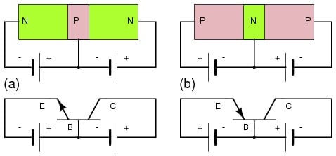
Note that the colored PNP and NPN diagrams are simplifications that don’t reflect the actual physical configuration of an integrated-circuit BJT.
NPN vs. PNP: Why PNP Transistors Matter
In my experience, NPN transistors spend much more time in the limelight than PNPs. A few reasons for this come to mind:
- The voltage and current behavior of an NPN transistor is (at least, in my opinion) significantly more intuitive.
- When a switch or driver circuit is required, NPNs provide a more straightforward interface to digital output signals (such as a control signal generated by a microcontroller).
- NPNs are actually better than PNPs in important ways. This has led to a particularly dominant position for the NPN because BJTs must compete with MOSFETs, and it’s easier for the BJT team to win when it sends an NPN into the match. The author of this 2009 UC Berkeley document, Chenming Hu, goes so far as to say that because of this situation—i.e., higher NPN performance and the general preference for MOSFETs—BJTs are “almost exclusively of the NPN type.”
So we can’t deny that PNPs are less common and, in general, less desirable—but that doesn’t mean we should ignore them. The rest of this article will discuss PNP characteristics and applications.
Charge Carriers: Electron vs. Hole
As shown above, a PNP transistor’s emitter and collector are formed via p-type doping. This means that most of the charge carriers in a PNP are holes.
This fact might seem irrelevant to practical engineering since we really don’t care what type of charge carrier is used as long as the circuit works. But it turns out that we can’t simply ignore the hole vs. electron issue because holes are “slower” than electrons. More specifically, they have lower mobility.
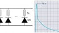
As shown in the following plot, electron mobility is always higher than hole mobility, though the doping concentration does influence the difference between the two. (Note that this plot is specifically for silicon.)

As you might have guessed, higher electron mobility gives NPN transistors a speed advantage over PNPs. The UC Berkeley document cited above indicates that the higher mobility also leads to higher transconductance, and higher transconductance means higher small-signal gain. I’m not sure about this, though. As far as I can tell, mobility has a significant effect only on MOSFET transconductance, not BJT transconductance. If I’m wrong, feel free to let me know in the comments section.
NPN vs. PNP IC Manufacturing
There is another reason why PNPs are less popular than NPNs, and it has to do with something that many electrical engineers never need to worry about: the actual process of manufacturing integrated circuits. I’ve seen various indications that NPNs are easier and/or cheaper to manufacture than PNPs, though it is difficult to find detailed (and authoritative) information on this topic.
I did find one solid explanation though, and it relates specifically to BiCMOS technology. My old Sedra and Smith textbook (Microelectronic Circuits) says that “most BiCMOS processes” were not able to produce optimized PNP transistors. IC designers who were working with BiCMOS apparently had to settle for non-optimized devices—or maybe “downright mediocre” would be a better way to describe them. The book indicates that the β was around 10 and the high-frequency performance was less than impressive; the BiCMOS NPN devices, in contrast, had β of 50 to 100 and could be used with frequencies up into the gigahertz range.
Implementation of PNP Transistors
The fundamental operation of PNPs is the same as that of NPNs, but the polarities are reversed in a way that sometimes leads to awkward circuit configurations.
- Current flows from emitter to base; the emitter must be ~0.6 V above the base in order to forward bias the base-emitter junction.
- Current flows out of the collector, and the collector voltage is lower than the emitter voltage.
- The common-emitter configuration, which is intuitive and straightforward with NPNs, becomes a little strange with PNPs because the “common” emitter is connected not to ground but to a positive supply rail.

Applications for PNP Transistor Circuits
My goal here is not to list all the circuits that could employ a PNP transistor. Actually, this would be impossible, since PNPs can be used in countless ways, though in many cases an NPN might be preferable. Instead, I’m going to highlight a few circuits or applications that I have noticed as common places to find a PNP transistor in action.
- A high-side current mirror or active load (such as the one used in my article on gain margin and phase margin).

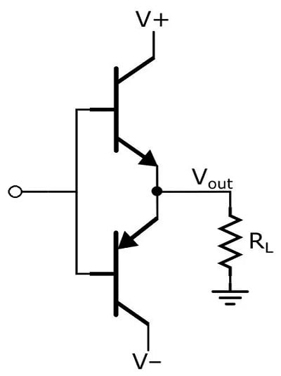
- Complementary driver/amplifier configurations, such as the Class B and Class AB output stages.
- Low-dropout regulators. Using a PNP instead of an NPN as the pass element gives the regulator a significantly lower dropout voltage, but it also increases the quiescent current (see this app note for more information).
- Driver applications where one side of the load is grounded. The emitter of the PNP is connected to the drive voltage, and the other side of the load is connected to the collector. This configuration is called a high-side switch; this AAC forum thread gives you an example and might include some helpful discussion.
Conclusion
We’ve explored the defining characteristics of PNP transistors, and we’ve also seen why NPNs are often preferred. Feel free to leave a comment if you have another example of a circuit or application that typically uses PNPs instead of NPNs.


I want to use PNP and NPN transistor for my circuit. I’m using eliminator for the power supply which can output 5v. This voltage is used for both the transistors.
Now the question is, can I use these two transistors continuously without any register or any other components for 24*7 or 365*7 ? Do I need to use heat sink? Or will transistors lose their life in a month if I use transistors like this?