 Facebook
 Google
 GitHub
 Linkedin
Purpose and Internal Functionality of FPGA Look-Up Tables
This article explains the Look-Up Tables (LUTs) constituting Field Programmable Gate Arrays (FPGAs).
This article explains the Look-Up Tables (LUTs) constituting Field Programmable Gate Arrays (FPGAs).
FPGAs and Their Internal Architecture
Field Programmable Gate Arrays (FPGAs) offer a reconfigurable design platform which makes them popular among digital designers. Typical internal structure of FPGA (Figure 1) comprises of three major elements:
- Configurable Logic Blocks (CLBs), shown as blue boxes in Figure 1, are the resources of FPGA meant to implement logic functions. Each CLB is comprised of a set of slices which are further decomposable into a definite number of look-up tables (LUTs), flip-flops (FFs) and multiplexers (Muxes).
- Input/Output Blocks (IOBs) available at FPGA’s periphery facilitate external connections. These programmable blocks carry signals ‘to’ or ‘from’ FPGA chip. Figure 1 shows IOBs as a set of rectangular boxes enclosed within the FPGA boundary (violet colored outer box).
- Switch Matrix (shown as red-colored lines in Figure 1) is an interconnecting wire-like arrangement within FPGA. These offer connectivity for the CLBs or provide dedicated low impedance, minimum delay paths (for example, global clock line).
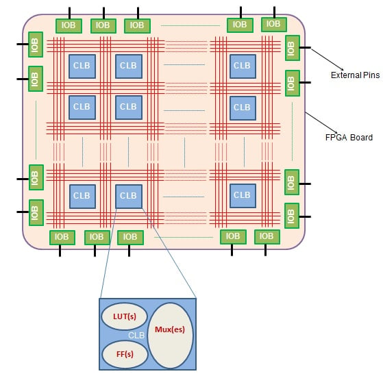
Figure 1: Internal architecture of a typical FPGA.
Overview of Look Up Tables (LUT)
One of the features which make FPGA families differ from each other is their logic resource. For example, each CLB of Spartan-II FPGAs (PDF) is comprised of two slices, each with two LUTs. The Spartan 6 (PDF) has two slices with four LUTs each. Internally, LUTs comprise of 1-bit memory cells (programmable to hold either ‘0’ or ‘1’) and a set of multiplexers. One value among these SRAM bits will be available at the LUT’s output depending on the value(s) fed to the control line(s) of the multiplexer(s).
The number of inputs available for a LUT determine its size. In general, a LUT with n inputs is seen to comprise of 2n single-bit memory cells followed by a 2n:1 multiplexer or its equivalent (say, two 2n-1:1 muxes followed by one 2:1 mux).
A specific example of a 2-input LUT comprising of 4 SRAM bits and a 4:1 mux is as shown in Figure 2a. Next, Figure 2b shows its equivalent architecture but represents a 4:1 mux as a tree of 2:1 muxes.
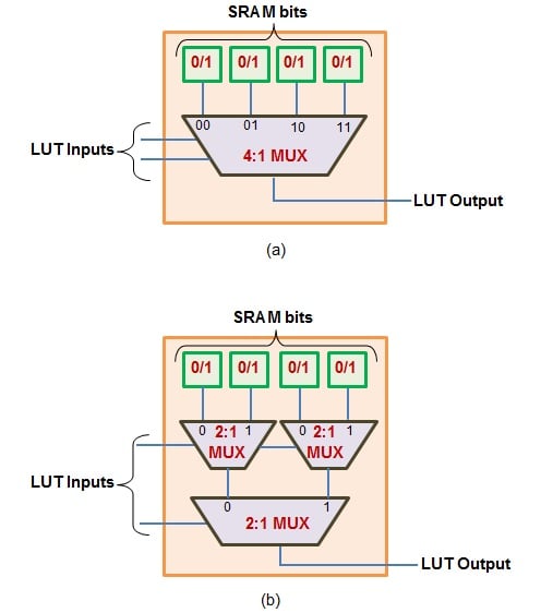
Figures 2(a) and 2(b): Internal structure of a 4-bit LUT
Implementation of Logic Functions using LUT
FPGA makes use of its LUTs as a preliminary resource to implement any logical function. This is actually a two-phase process.
At first, the output values for each combination of input variables constituting the Boolean Function are stored in the SRAM cells of the LUT. After this, depending on the combination of input variables supplied by the user, the appropriate memory bit will appear at LUT’s output pin. This is due to the fact that the user-provided input bits act as the select lines for the multiplexer(s) present inside the LUT(s).
Case 1: Number of Input Variables are Equal to the Number of LUT Inputs
Suppose we want to realize a Boolean Function of four input variables A, B, C and D using a 4-input LUT. Here, let the output become high only when any of the two input variables are one. The truth table corresponding to this is shown below.
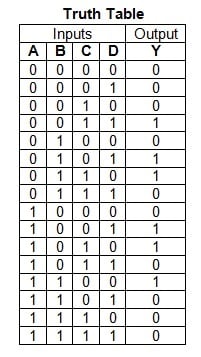
While realizing this function using an FPGA, A, B, C, and D will be the inputs to LUT. Next, the values of the output variable for each of their combination (available in the last column of the truth table) will be stored in the SRAM cells, as shown in Figure 3.
Now, if ABCD = 0101, then the output of the LUT, Y, will take the value of 1 as the content of the sixth memory cell makes its way to the output pin (as shown by the red discontinuous line in Figure 3).
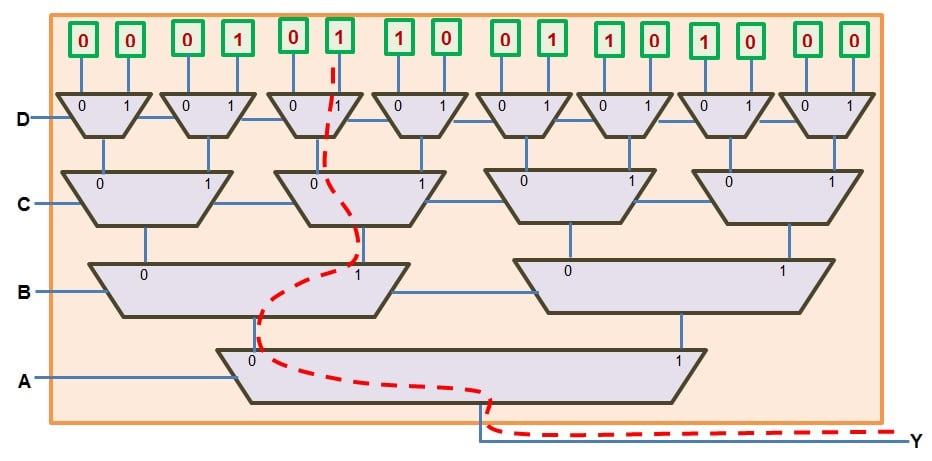
Figure 3: Implementation of 4-input Boolean function using 4-input LUT
Case 2: Number of Input Variables is More Than the Number of LUT Inputs
What do we do when our FPGA does not have a 4-input LUT, but only 3-input LUTs? Can we implement our function in it? Yes, we can.
Figure 4 shows this mode of realization. Here, two 3-input LUTs share the same set of three lower-significant inputs (B, C, and D). The output from any one of these LUTs is routed onto the Y output bit (shown by a red discontinuous line) using a 2:1 mux whose select line will be our fourth variable, A (MSB).
In this illustration, the last 2:1 mux is considered to be the multiplexer present within the slice constituting the CLB.
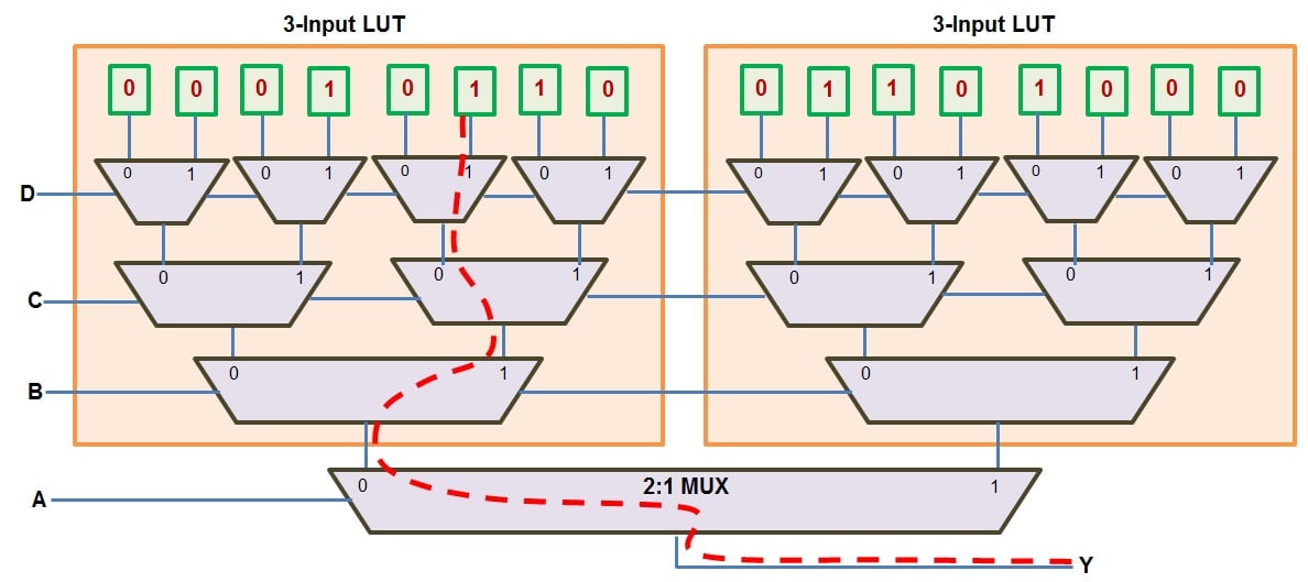
Figure 4: Implementing a 4-input Boolean function using a combination of 3-input LUTs and a Mux
Case 3: Number of Input Variables is Less Than the Number of LUT Inputs
Now, imagine that we have an FPGA comprising of 4-input LUTs in which we need to realize a 3-input logic function.
In this case, three input variables constituting the Boolean expression drive the three (LSB) inputs of the LUT while its fourth input (MSB) will be pulled low. Then, 8 SRAM cells are configured to hold the output values of the function while the other eight cells are set to zeros.
For example, Figure 5 shows a possible way of a realizing the sum output of a full adder using a 4-input LUT. Here, the path traversed (a red discontinuous line) shows the case for ABC = 011 for which the output Y becomes 0.
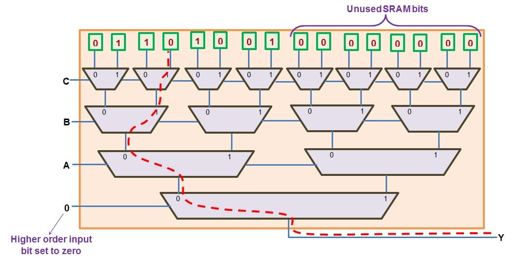
Figure 5: Realization of a 3-input logic function using 4-input LUT
Analysis of the cases presented leads us to conclude that FPGAs can effectively implement any of the combinatorial design using the FPGA's LUTs in conjunction with additional components like muxes, whenever necessary.
On the other hand, if we need to implement sequential circuits, then in addition to the multiplexers, even the flip-flops present within the slices would need consideration. In fact, this is the way in which FPGAs realize almost all of our Boolean expressions, irrespective of their complexity.
The Importance of LUTs
Assume that we have to compute a trigonometric function, such as computing the cosine, of a discrete input variable spanning a definite range. When done directly, cosine must be computed for each and every input. This process would be computationally expensive and thus inefficient particularly if the range is large.
Instead, we can pre-compute the cosines for all the possible inputs within the range and store them in a LUT. After this, computing the cosine for any input value would involve the action of fetching (not computing) the corresponding value from the look-up-table. This would greatly reduce the run-time, making it much more efficient.
In addition, note that the SRAM cells of the LUTs are one of the important factors which contribute to the reconfiguring ability of the FPGAs. This is because the configuration bits constituting them can be changed each time the device is powered-up, which in turn changes their functionality.
For example, the LUT acting as an adder can be made to behave as a subtractor just by changing the values stored in its SRAM cells (PDF). However, we should not forget that almost all LUT-based operations are prone to glitches.
Related Content


Simple yet I learned many new things. Thank you very much for this important information.
I have a question related to the last paragraph.
—To pre-compute the cosines for all the possible inputs within the range, we need a computer & then we save the output in LUTs. So, aren’t we using the same resources in both methods i.e calculating either with computer or with FPGAs because ultimately we used computer to calculate all the possible inputs in both cases. Kindly explain.