Facebook
 Google
 GitHub
 Linkedin
Getting Started with FPGAs: Lookup Tables and Flip-Flops
Dive under the hood of an FPGA: Just what is inside of an FPGA that makes it so different from a microcontroller and yet still so versatile?
Just what makes an FPGA so different from a microcontroller and yet so versatile? This article continues the exploration of FPGAs, focusing on the role of flip-flops and lookup tables (LUTs) in logic blocks.
The fundamental building blocks inside of an FPGA are the flip-flop and the lookup table (LUT). These are combined to form what are referred to as logic blocks. The logic blocks connect to each other, and the outside world, through programmable interconnects. The flip-flops operate more or less like any flip-flop you may have stumbled upon over the years. LUTs, on the other hand, aren’t quite as universal a concept.
Supporting Information
Previous Articles in This Series
- A Microcontroller Enthusiast’s First Look at Programmable Logic
-
Getting Started with FPGAs: The Development Environment and “Hello World”
FPGA Internals
Before I understood anything about the internal workings of the FPGA, I wondered how the devices could be loaded up with all of the random gates needed to create a working logic device. That’s a reasonable question to ask, but I should have thought of the lookup table. I’ve used them in other settings, myself.
If you take a look at the datasheet for a logic gate, you’ll find a truth table. It’s pretty simple. Put a specific combination of ones and zeros on the input lines, and either a one or a zero comes out the other end.

The LUT in an FPGA holds a custom truth table, which is loaded when the chip is powered up. Think of the LUT as a small scratchpad RAM. The LUT inputs act as the address lines for a corresponding one-bit-wide RAM cell. When an FPGA is configured, the bits of the LUT are loaded with ones or zeros based on what the desired truth table would be. Instead of wiring up a bunch of logic gates that create the desired truth table, it’s just simulated in a special type of RAM.
A conventional two-input logic gate provides a specific output for four different input combinations, and thus it could be simulated with a 4×1 bit scratchpad RAM. A four-input LUT would take a 16×1 bit scratchpad RAM.

The logic blocks in the FPGA I’m using in this article, the Xilinx Spartan 6 LX9, have 64×1 RAM cells, each accompanied by a dual flip-flop. The LUTs are set to mimic logic gate combinations, and the flip-flops are used as a form of storage and as counters and dividers. The combination LUT/dual flip-flop can be used as “logic, distributed RAM, or shift-registers,” as stated in the "Spartan-6 Family Overview", linked above. Many FPGAs also have larger banks of RAM, called block RAM, which can only be used for storage. More specific detail on this chip can be found in the overview document linked to above.
What all that means in practice is that our hardware description language (HDL) code configures sets of these logic blocks to provide all of the functionality we need from an FPGA.
One Caution with LUTs
One disadvantage of the LUT is a phenomenon referred to as a "glitch." It’s not a “glitch” in terms of any generic thing gone wrong, but a specific characteristic of LUT-based logic.
Consider a discreet logic gate. You put logic ones or zeros on the inputs and the output almost instantly changes. There will be a bit of propagation delay, but there’s never any ambiguity in terms of what the output is. Change the inputs of a two-input AND gate from "zero, zero" to "one, one" and the output is guaranteed to go from zero to one.
In a LUT, however, you’re really changing the address on a one-bit wide RAM bank. There can be a brief moment when the LUT input bits change—the RAM address is being changed—when the RAM effectively doesn’t know what to put on the output. If, in that period of uncertainty, the LUT output differs from what the intended output is, we call that a glitch.
With discrete logic chips, you can perform operations asynchronously: just do something on the input and the change will propagate all the way through your set of logic gates. However, with LUTs, your intended output may not be accurate until the glitch period is passed.
Glitches aren’t a problem in today’s example, but it’s good to start with some awareness. Dealing with them will be covered in a later article in this series.
Back to the Development Board
In my last installment, I chose a development board, installed the development environment, and synthesized and loaded a simple LED flashing “Hello World” FPGA configuration. In this article, I’m going to explore a bit of what that configuration looks like under the hood, and continue down the path of clarifying differences between microcontrollers and FPGAs.
But first, I’m going to add a bit more hardware to help illustrate what’s going on. I need one pushbutton switch and four LEDs (five if you include the onboard LED1). The pushbutton will be used to enable the counting, and the LEDs will display output from parts of the register.

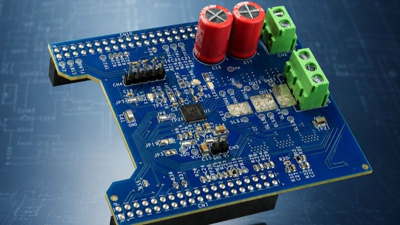
Shown is my Papilio Pro with a button/LED wing. I’m using all four LEDs, but only one of the push buttons.
You can repeat the steps in my prior installment to create a new project, but use the name “RegisterCounting” as the project and file names instead of “HelloWorld.”
The UCF and Ports
The complete, new, UCF code follows:
NET clk_in        LOC = P94   | IOSTANDARD=LVTTL | PERIOD=31.25ns;

NET reset         LOC = P121  | IOSTANDARD=LVTTL | PULLDOWN;

NET ExtLEDs<0>    LOC = P112  | IOSTANDARD=LVTTL | DRIVE = 8 | SLEW = SLOW ;
NET ExtLEDs<1>    LOC = P120  | IOSTANDARD=LVTTL | DRIVE = 8 | SLEW = SLOW ;
NET ExtLEDs<2>    LOC = P118  | IOSTANDARD=LVTTL | DRIVE = 8 | SLEW = SLOW ;
NET ExtLEDs<3>    LOC = P116  | IOSTANDARD=LVTTL | DRIVE = 8 | SLEW = SLOW ;
NET ExtLEDs<4>    LOC = P114  | IOSTANDARD=LVTTL | DRIVE = 8 | SLEW = SLOW ;
The first line of the UCF is unchanged from my prior version. It creates a label for the clock signal that enters the chip at pin P94.
Following that, I’ve created the label “reset” for button number 1 on the wing. Button 1 is wired to chip pin P121. It isn’t designated as an input or output here in the UCF. That takes place in the module declarations section of the Verilog code, which you’ll see shortly. The parameter at the end of its line, “PULLDOWN”, is accurately descriptive—a pulldown resistor will be connected to chip pin P121.
The next part illustrates one of the prime concepts that can be problematic for those who are accustomed to working with microcontrollers. “ExtLEDs” looks like a rather conventional array, but it’s not.
In the UCF, we’re labeling connections (the programmable interconnects) to chip pins that connect to the outside world. NET “ExtLEDs” is more akin to a set of signal wires coming from a microcontroller I/O port than to an array. The code to put data into ExtLEDs, or to access each individually, looks similar to that used to manipulate a software array. However, each member of ExtLEDs just represents a signal wire that will be used as a connection to a certain bit in a register. In FPGA terminology, each of these members that we are referring to in the UCF are properly called signals. ExtLEDs is a set of five signals that can be referenced as a group.
You may notice that P112 is the same chip pin as the onboard LED we used in the prior article. It is. With ExtLEDs, we’re simply defining a set of signals, and we’re assigning labels to them. There is no need for the pins to be sequential or even in physical proximity. The other chip pins connected with ExtLEDs are wired to pins on the I/O connector, which connect to the LEDs on the button/LED wing I have installed.
The Expanded Verilog
The Verilog code follows:
`timescale 1ns / 1ps

module RegisterCounting(
        input wire reset,
        input wire clk_in,
        output wire [4:0] ExtLEDs
   );

    reg  [25:0] freq_div;                  // 26-bit register that I will be using as the frequency dividing counter

    assign ExtLEDs[4:0] = freq_div[25:21]; // connects the 4 led outputs to register bits at 25, 24, 23, and 22

    always @(posedge clk_in) begin         // Clocked on the rising clock edge
        if(reset)                          // Restart the counter at 0, if the button is pressed
             freq_div <= 0;
        else
            freq_div <= freq_div + 1'b1;   // Increment the register by 1

    end

endmodule
In the module declaration, reset and clk_in are defined as inputs. The five-bit signal “ExtLEDs” is declared to be an output.
I’ve expanded the register “freq_div” to 26 bits (in the previous article it was defined with 21:0, which is 22 bits wide). The onboard LED still shows the value in bit 21 of the register, and the four LEDs on my Papilio wing show the value in bits 22:25. Each bit will flash at half the frequency of the prior bit.
In the next statement, “assign ExtLEDs[4:0] = freq_div[25:21];”, the five signals (4:0) from “ExtLEDs” are connected to five of the bits (25:21) in the register “freq_div.”
That’s cause for another confusion alert. If you’re thinking in MCU code terms, you might interpret that assignment as happening when that line of code is executed. That would not be correct. The assign statement is creating a steady connection between those register bits and the outputs.
I tend to visualize the Verilog “assign” statement as something along the lines of connecting a wire. In this case, it’s a five-wire ribbon cable between the five output signals in “ExtLEDs” and the five most significant bits in the register “freq_div.” Those connections will be formed in the FPGA at power-up and will always be active.
That means two things:
- One, it doesn’t matter much where in the code you put the assign statement. The routing takes place during the synthesis step, not at execution time. The statement is just as valid if it’s at the end of the code. You can prove that by moving that assign statement down to just above the “endmodule” line.
- Two, no matter where in the HDL code you set a value in the register, it will instantly appear on those outputs. You don’t need to assign again, as you would in an MCU language. Even if your assign statement is at the bottom of your code, that signal is still accessible just about anywhere else in the code.
Numeric Notation
In my prior article, I used a slightly different notation in the line to increment the register. In this article’s code, I use (freq_div <= freq_div + 1'b1;), whereas in the previous article I used the numeric notation 1’d1. Both are technically correct, but as commenter Bill pointed out, 1’b1 is more correct.
The first number in the notation refers to the number of bits used to store the value—the register bit width. For example, 1’b1 creates a register that is one-bit wide and puts the number 1 in it, and 4’b1 creates a four-bit wide register and puts the number 0001 in it. The “b” indicates the radix (or base) for the trailing number, in this case, binary; “d,” “h,” and “o” represent decimal, hexadecimal, and octal, respectively. It’s not case sensitive, so d equals D.
That first number means the same thing, regardless of the radix. 1’d1 creates a one-bit register with the number 1 in it. 4’d1 creates a register with 0001, as does the notation 4’b1. The first number always represents the bit width of the register. The radix indicates the number set you are using for the number, and the trailing number is the value.
Here’s where my use of 1’d1 is technically correct, but can lead to trouble. The notation 1’d2 still creates a one-bit register. That works fine to represent the value 1. But, since the binary for 2 is 10, the MSB is dropped, leaving just the 0. 1’d2 will equal zero. 1’d3 equals 1, and 1’d4 equals zero again.
Summary
Examining the use of lookup tables, flip-flops, and programmable interconnects goes a long way toward understanding how an FPGA works.
Logic is created in the LUT. Flip-flops are used to create registers, which store data. The programmable interconnects route the data signals from logic and registers to the outside world.