Facebook
 Google
 GitHub
 Linkedin
Synchronous Demodulation Using Analog Multipliers vs. Switch-based Multipliers
In this article, we’ll look at the pros and cons of using a switch-based multiplier.
In a previous article, we looked at the basics of the synchronous demodulation technique. This technique is helpful for measuring a low-frequency signal that is buried in the flicker noise. It attempts to operate the circuit at a frequency sufficiently higher than the 1/f corner frequency of the circuit so that the flicker noise is no longer a limiting factor.
The synchronous demodulation technique can be implemented using either an analog multiplier or a switch-based multiplier. From an implementation point of view, the switch-based multiplication is more convenient.
In this article, we’ll look at the pros and cons of using this type of multiplier.
Synchronous Demodulation Using Analog Multipliers
Figure 1 shows a basic block diagram for implementing the synchronous demodulation technique.
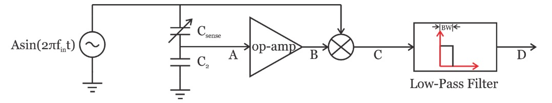
Figure 1
Assuming that the output signal of the op-amp is \(v_B(t)=Bsin(2\pi f_{in}t+ \phi)\), we obtain:
\[v_C(t)=Asin(2\pi f_{in}t) \times Bsin(2\pi f_{in}t+ \phi)= \frac {1}{2}ABcos(\phi)-\frac {1}{2}ABcos(4\pi f_{in}t+\phi)\]
The second term is at twice the input frequency and is suppressed by the low-pass filter. So we have:
\[v_D(t)= \frac {1}{2}ABcos(\phi)\]
If we assume that the op-amp is not introducing any delay, i.e. \(\phi=0 \), we obtain \(v_D(t)= \frac {1}{2}AB\). Therefore, the output of the low-pass filter is proportional to the amplitude of the signal at node A and can be used to measure the value of \(C_{sense}\).
The above design has one major shortcoming: it needs an analog multiplier.
Analog multipliers, such as the Gilbert cell, usually have linearity problems. (For more information, please refer to Section 10.3 of this book.)
Instead of using an analog multiplier, we can use switch-based circuitry to perform the required multiplication.
In this article, we’ll examine the basic concept of multiplying by a square wave and comparing its noise performance to that of a synchronous demodulation system that uses an analog multiplier.
Synchronous Demodulation Using Square Waves
The block diagram of the square wave-based synchronous demodulator is shown in Figure 2. A “Zero-Crossing Detector” is used to convert the input sine wave into a square wave that drives the switch SW.
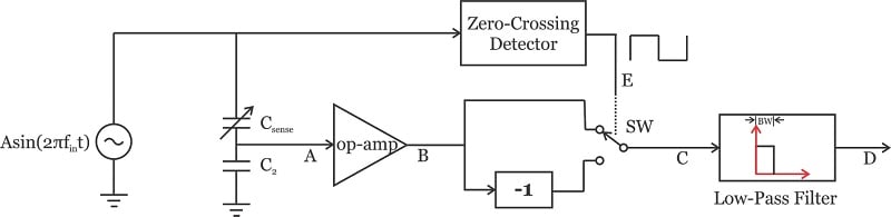
Figure 2
Since the square wave is generated from zero crossings of the sine wave, both waveforms are of the same period (as depicted in Figure 3).
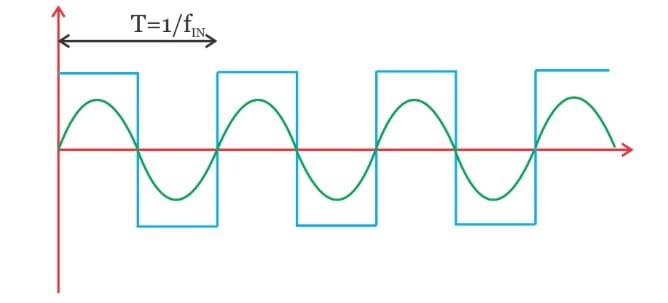
Figure 3
When the square wave is high, the output signal of the op-amp is directly applied to the low-pass filter; however, when the square wave is low, the signal experiences a gain of -1 before it reaches the low-pass filter. Effectively, the op-amp output is multiplied by the square wave.
The Fourier analysis reveals that the spectrum of the above square wave consists of sinusoids at the odd harmonics of the square wave fundamental frequency. Assuming that the high and low values of the waveform are respectively 1 and -1, we get the following:
\[v_{squarewave}(t)=\sum^\infty_{n=1, 3, 5} \frac {4}{n\pi}sin(2 \pi nf_{IN}t)\]
When we multiply a sine wave with frequency \(f_1\) by another sine wave with frequency \(f_2\), we obtain two cosine terms at the sum \((f_1+f_2)\) and difference \((f_1-f_2)\) frequencies. Multiplying \(v_B(t)=Bsin(2\pi f_{in}t+ \phi)\) by each frequency component of the square wave will lead to two frequency components at the corresponding sum and difference frequencies. You can see the results of this in Figure 4.
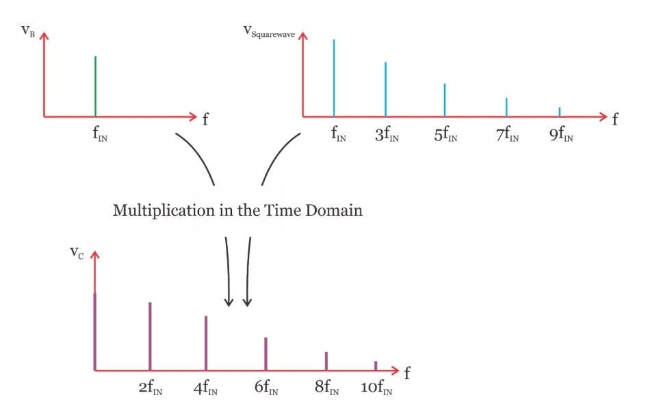
Figure 4
As you can see, we have a DC term along with frequency components at the even harmonics of the sensor excitation frequency. The high-frequency components will be suppressed by the narrow low-pass filter and there will remain only a DC term that can be used to extract the value of \(C_{sense}\).
Note that the output frequency component at \(2f_{IN}\) originates from two different multiplications: the sum frequency term of multiplying \(v_B(t)\) by the first harmonic of the square wave \((f_{IN}+f_{IN}=2f_{IN})\) and the difference frequency term of multiplying \(v_B(t)\) by the third harmonic of the square wave \((3f_{IN}-f_{IN}=2f_{IN})\). Similarly, each of the output frequency components at \(4f_{IN}, 6f_{IN},\cdots \) originates from two different multiplications.
Noise Performance of Multiplying by a Square Wave
The synchronous demodulation shown in Figure 2 replaces an analog multiplier with a switch and some other blocks. We’ll see that the circuit implementation of this new method is much easier than the analog multiplier-based method.
With a square wave-based demodulator, however, the input is multiplied by all of the odd harmonics of the sensor excitation frequency.
Can these unwanted multiplications increase the noise at the output of the low-pass filter?
To better understand why one should worry about these unwanted multiplications, consider the spectra shown in Figure 5.
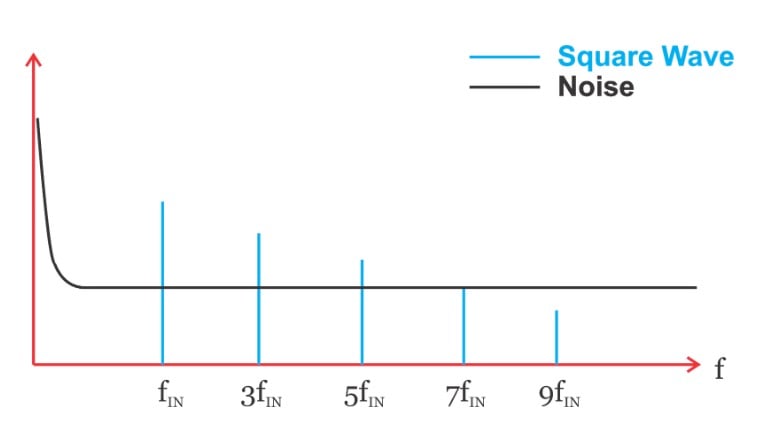
Figure 5
In this figure, the black curve shows the frequency content of the noise at node B, whereas, the blue lines depict the spectrum of the square wave.
When these two signals are multiplied in the time domain, a given frequency component of the square wave \((nf_{IN})\) will shift the noise spectrum both to the right and the left by \(nf_{IN} \) (just as the multiplication of two sine waves produced frequency components at the sum and difference frequencies of the two input sine waves).
After the multiplication, we have the low-pass filter. This means that only part of the noise that is frequency shifted to DC and lies in the pass-band of the filter will remain and the other noise components will be suppressed.
What noise components are going to be downconverted to DC? The answer is: only regions of the noise profile that are close to a frequency component of the square wave (the colored regions in Figure 6).
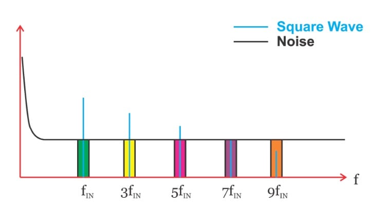
Figure 6
An ideal square wave consists of an infinite number of frequency components at odd harmonics. Theoretically, there is an infinite number of noise regions that are frequency shifted to DC.
Does this mean that the noise of the square wave-based approach will be unacceptably high?
Surprisingly, multiplication by the square wave shown in Figure 3 will not increase the noise at DC (see the proof below). When the square wave is high, the noise at node B is directly transferred to node C; when the square wave is low, the noise is transferred with a gain of -1.
When analyzing the noise effect, we are interested in its power (that mathematically involves a square operation). As a result, the gain of -1 for the low state of the square wave can be ignored and we can assume that, for the whole period of the square wave, the noise at node B is transferred to node C.
Based on this observation, we know that the total noise power at the output of the square-wave based multiplier is the same as the total noise power at its input. However, this intuitive argument does not reveal how much noise we’ll have at DC after the multiplier. (Note that we are interested in the low-frequency noise because the low-pass filter will reject the other noise components.)
The mathematical analysis of the next section can give us a better understanding of the noise performance of the square wave-based multiplier.
Mathematical Analysis of the System Noise
We discussed that only regions of the noise profile that are close to a frequency component of the square wave (the colored regions in Figure 6) can be downconverted to DC. Figure 6 suggests that if \(f_{IN}\) is sufficiently larger than the 1/f corner frequency, the flicker noise will not contribute to the noise power at the output of the low-pass filter. For calculating the noise power at the output of the low-pass filter, we can ignore the flicker noise.
Given that, we assume that the noise power spectral density (PSD) is flat and has a one-sided value of η at all frequencies (as shown in Figure 7(a) below). With one-sided representation, the noise power at the negative frequencies is folded around the vertical axis and added to the power in the positive frequencies.
For a real signal, the PSD is an even function, therefore, the equivalent two-sided PSD for the spectrum in Figure 7(a) will be as shown in Figure 7(b) (the negative frequencies are included but the PSD value is halved).
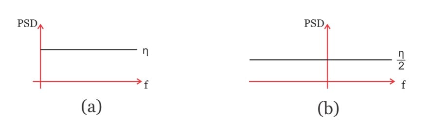
Figure 7
With the flat spectrum in Figure 7(b), we can more easily calculate the output noise because shifting the PSD either to the right or to the left will not change it. Let’s examine the effect of the n-th frequency component of the square wave, e.g. \(v_{squarewave, n}(t)=\frac {4}{n\pi}sin(2\pi nf_{IN}t)\), on the PSD depicted in Figure 7(b). This term can be rewritten as:
\[v_{squarewave, n}(t)=\frac {4}{n\pi} \times \frac {e^{j2\pi nf_{IN}t}-e^{-j2\pi nf_{IN}t}}{2j}\]
The terms \(e^{\pm j2\pi nf_{IN}t}\) will frequency shift the PSD, but can be ignored because the PSD is flat. These shifted PSDs will experience an attenuation factor of \(A= \pm \frac {4}{j2n\pi}\). We know that applying a noise with PSD of \(S_{input}(f)\) to a system with a transfer function of H(f) leads to a noise PSD of \(S_{input}(f) \times |H(f)|^2\) at the system output (Please see this article). Therefore, the n-th component of the square wave will lead to the following two-sided PSD at the output:
\[PSD_{out,n}= \frac {\eta}{2} \times \left ( \left |+\frac {4}{j2n\pi} \right |^2 + \left | -\frac {4}{j2n\pi} \right |^2 \right )= 2 \times \frac {\eta}{2}\times \left ( \frac {4}{2n\pi} \right )^2 =\frac {\eta}{2} \times \frac {8}{(n\pi)^2}\]
The total noise will be the sum of the \(PSD_{out,n} \) terms for all odd values of n. This gives us:
\[PSD_{out}=\sum^{\infty}_{n=1, 3, 5} \frac {\eta}{2} \times \frac {8}{(n\pi)^2}= \frac {\eta}{2} \times \frac {8}{(\pi)^2} \sum^{\infty}_{n=1, 3, 5}\frac {1}{n^2}\]
It can be shown that
\[\sum^{\infty}_{n=1, 3, 5}\frac {1}{n^2} = \frac {\pi ^2}{8}\]
So now we have
\[PSD_{out}= \frac {\eta}{2}\]
As you can see, assuming that the PSD at node B is flat, the square wave-based multiplier does not change the PSD value or shape.
What About Other Noise Sources?
Considering the above discussion, the output PSD of a square wave-based multiplier with a flat input noise spectrum is the same as that of the input noise. However, a square wave-based synchronous demodulator can still have an inferior noise rejection compared to a system that uses an analog multiplier.
As an example, assume that a strong noise component at 3 kHz appears at the output of the amplifier in Figure 2. If we use a sensor excitation frequency of \(f_{IN} =1 KHz\) , the third harmonic of the square wave will coincide with the noise frequency. The noise will be downconverted to DC and will appear at the output of the low-pass filter.
This means that, when using a square wave-based demodulator, we have to consider the potential noise components (such as the harmonics of the power line frequency) and choose an appropriate excitation frequency for the sensor.
Conclusion
The synchronous demodulation technique can be implemented using either an analog multiplier or a switch-based multiplier. From an implementation point of view, the switch-based multiplication is more convenient.
If we apply a flat noise PSD to a switch-based demodulator, the output PSD will be the same as the input. The noise performance of a square wave-based demodulator should not be inferior to that of an analog multiplier-based system. However, we have to choose an appropriate excitation frequency for the sensor so that other known noise sources (such as the power line harmonics) do not coincide with the odd harmonics of the square wave.
The next article will take a look at the practical implementation of a square wave-based synchronous demodulator.
To see a complete list of my articles, please visit this page.