Facebook
 Google
 GitHub
 Linkedin
Analog and Digital Implementation of a Synchronous Demodulator
In this article, we’ll take a look at the analog blocks for implementing the square wave-based synchronous demodulator.
In previous articles of this series, we discussed the basics of the synchronous demodulation technique.
In this article, we’ll take a look at the analog blocks for implementing the square wave-based synchronous demodulator. We’ll also briefly look at the FPGA implementation of the synchronous demodulation technique.
Square Wave-Based Synchronous Demodulator
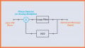
The block diagram of the square wave-based synchronous demodulator is shown in Figure 1.
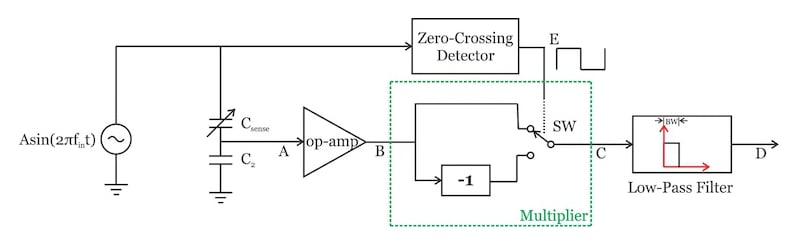
Figure 1. Square wave-based synchronous demodulator
The two blocks that we’ll examine are the “zero-crossing detector” and the “multiplier.”
Zero-crossing Detector
The “zero-crossing detector” converts the input sine wave into a square wave that drives the switch SW. This can be done using the circuit in Figure 2.
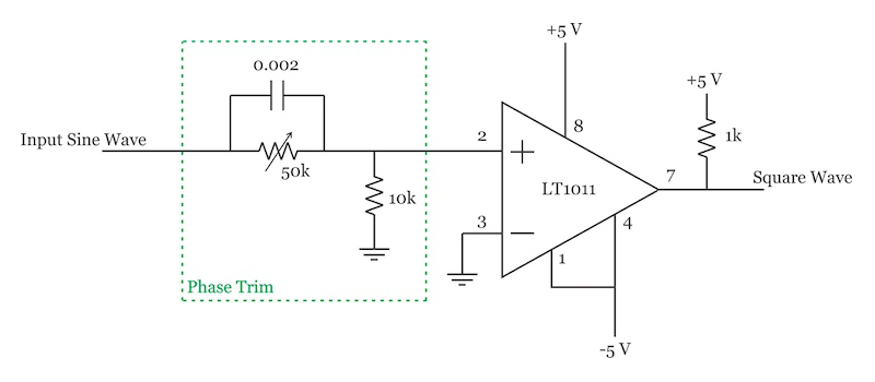
Figure 2. The zero-crossing detector block in a synchronous demodulator. Schematic used courtesy of Linear Technology
The LT1011 is a voltage comparator that compares the input sine wave with the ground level. The potentiometer is used to adjust the phase of the produced square wave so that it matches the phase of the sine wave at node B in Figure 1.
In this way, we can have a square wave that switches when the sine wave crosses 0 V. Recall that the signal amplitude at the output of the multiplier is a function of the phase difference between the two inputs of the multiplier. When the square wave is in phase with the sine wave, the phase relationship between the two signals is known and we can more easily interpret the voltage that appears at the output of the low-pass filter.
Multiplier
One common implementation for the “Multiplier” block is shown in Figure 3:
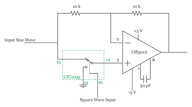
Figure 3. The multiplier block of the example synchronous demodulator. Schematic used courtesy of Linear Technology
In this figure, the LM301A is a general-purpose operational amplifier. The LTC1043 is a building block originally designed for implementing discrete switched-capacitor circuits. Figure 4 shows a simplified block diagram of a portion of the circuitry inside the LTC1043.
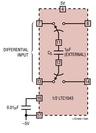
Figure 4. Diagram of the LTC1043. Image courtesy of Linear Technology
As shown in this figure, the differential input is connected to an external capacitor during the sampling phase. During the next phase, the charged capacitor is connected to the output port. The clock for the switches can be created either internally or through an external CMOS clock.
This apparently simple functionality allows us to use the LTC1043 in a variety of applications such as precision instrumentation amplifiers and switched-capacitor filters. However, with the schematic shown in Figure 3, the LTC1043 is actually used as a simple switch.
Let’s see how this circuit can multiply the input by a square wave. When the switch connects terminals 12 and 14 together, we have the following schematic.
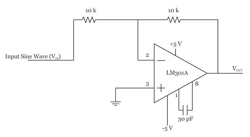
Figure 5
In this phase of operation, we have an inverting amplifier with a gain of \(\frac {V_{OUT}}{V_{IN}} = -1\). However, when terminals 12 and 13 of the LTC1043 are connected together, we obtain the following schematic:
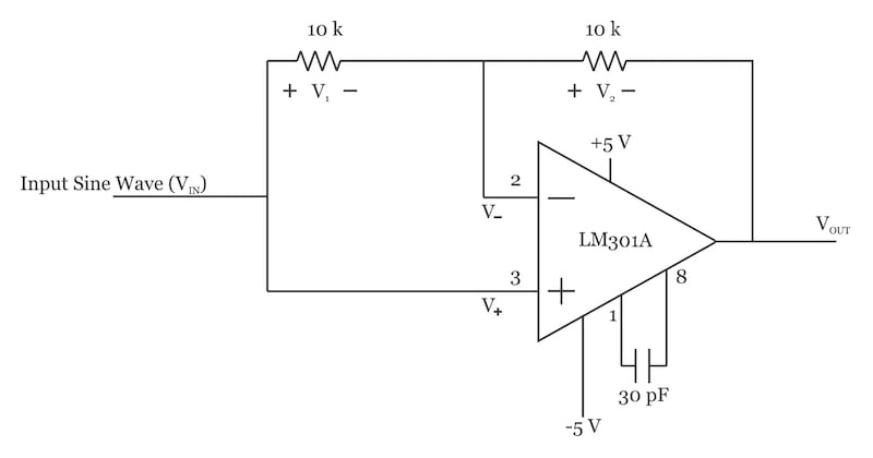
Figure 6. Connecting terminals 12 and 13 of the LTC1043
We know that due to the negative feedback path and the high gain of the op-amp, the two inputs of the op-amp have almost the same voltage: \(V_- = V_+\). Therefore, \(V_1 = 0 V\) and no current flows through the 10 kΩ resistor on the left.
Assuming that the current drawn by the op-amp inputs is negligible, the current through the 10 kΩ resistor in the feedback path will be zero as well and we have \(V_2 =0 V \). Therefore, in this phase of operation, we have a gain of \(\frac {V_{OUT}}{V_{IN}} = +1\). In other words, the input is multiplied by a square wave that toggles between ±1.
Digital Implementation of Synchronous Demodulation
Rather than using analog building blocks, we can use digital circuits to implement a synchronous demodulator. The basic idea is shown in Figure 7.
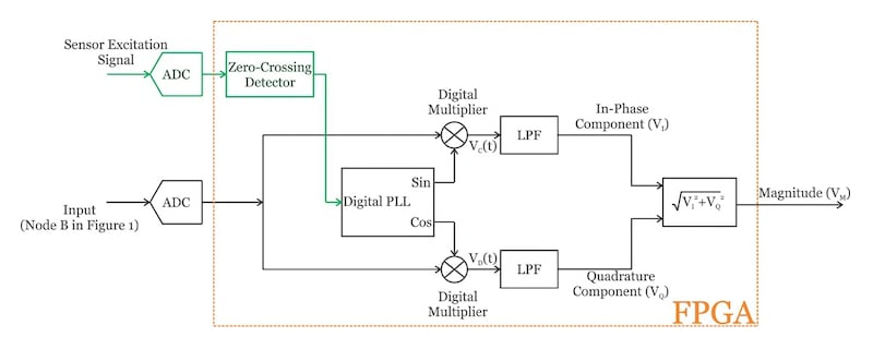
Figure 7. A digital synchronous demodulator circuit
Two A/D converters (ADCs) are used to digitize the input signal (node B in Figure 1) and the sensor excitation sine wave. As shown in the figure, the other blocks are digital and can be implemented by an FPGA.
In-phase and Quadrature Components
In Figure 7, the digitized input is multiplied by sine and cosine waves produced by a digital phase-locked loop (PLL). Why do we need to multiply the input by both the sine and cosine waves? In the first part of this series, we examined multiplication by a sine wave. If we multiply \(v_B(t)=Bsin(2 \pi f_{in}t+ \phi)\) by \(Asin(2 \pi f_{in}t)\), we obtain:
\[v_C(t)=Asin(2\pi f_{in}t) \times Bsin(2\pi f_{in}t+ \phi)=\frac {1}{2}ABcos(\phi)-\frac {1}{2}ABcos(4\pi f_{in}t+ \phi)\]
The first term is DC, however, the second term is at twice the input frequency. Hence, a narrow low-pass filter (LPF) can remove the second term and we have:
\[v_I=\frac {1}{2}ABcos(\phi)\]
The output is a function of the phase difference between the two inputs. This equation shows that a phase difference between the measured signal and the reference input can reduce the signal amplitude at the output of the LPF.
Additionally, we need to know the phase difference to be able to calculate the amplitude of the measured signal. (Remember that the analog solution discussed above used the “phase trim” circuitry to make the phase difference equal to 0). To circumvent these two problems, we incorporate a second multiplication stage that multiplies the input by a cosine wave:
\[v_D(t)=Asin(2\pi f_{in}t) \times Bsin(2\pi f_{in}t+ \phi)=\frac {1}{2}ABsin(\phi)+\frac {1}{2}ABsin(4\pi f_{in}t+ \phi)\]
After the LPF, we have:
\[v_Q=\frac {1}{2}ABsin(\phi)\]
We can calculate the magnitude of the input by taking the square root of the sum of the squares of the in-phase and quadrature components:
\[v_M= \sqrt{{v_I}^2+{v_Q}^2}= \frac {1}{2}AB\]
As you can see, the result is not a function of the phase difference.
Digital PLL
It is important to note that the digital PLL in Figure 7 must generate samples of sine and cosine waveforms. We can accomplish this by using a PLL that has a direct digital synthesizer (DDS) as its digitally controlled oscillator (DCO). The basic idea is shown in Figure 8.
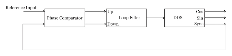
Figure 8. A PLL with a direct digital synthesizer. Image adapted from Cornell University
You can find more information about FPGA implementation of a synchronous demodulator here.
Conclusion
In this article, we examined both the analog and digital implementation of the synchronous demodulation technique:
For the analog implementation, we need a “zero-crossing detector” and a “multiplier”.
For the digital version, we can use two ADCs to digitize the measured signal and the sensor excitation waveform.
The other blocks can be implemented in an FPGA. By implementing both the in-phase and the quadrature paths, we can make the measurement independent of the phase difference between the multiplier inputs. For the digital implementation, we need a PLL that generates samples of sine and cosine waveforms. This can be achieved by a PLL that uses a DDS as a programmable oscillator.
Related Content