Facebook
 Google
 GitHub
 Linkedin
Understanding the PDK Generation Process
In this article, we'll walk through the steps of generating a Process Design Kit (PDK) for digital standard cell libraries.
Foundry manufacturers release a collection of files called the Process Design Kit (PDK) for each of their technology nodes. A full PDK encompasses the following:
- Back-end-of-line (BEOL) interconnect parasitic data.
- SRAM and logic standard cell characterization data.
- Design rules for BEOL and standard cell layers.
The PDKs play a vital role in providing the necessary models for RTL design simulation, evaluating power-performance-area (PPA) metrics, and creating manufacturable layouts. This article focuses on generation of a PDK for standard cell logic gates. Note that characterization of SRAMs and the development of memory compilers are beyond the scope of this article.
Back-End-of-Line (BEOL) Stack Definition
The first step in the PDK generation process is to define the BEOL stack. This includes the number of metal layers and via layers, the conductor and dielectric materials, and the metal and via geometries appropriate for the technology node.
Once the BEOL stack is defined, the electrical behavior of each layer is simulated and populated into a BEOL parasitic file. Synopsys EDA tools use Interconnect Technology Format (ITF) to describe the via resistances and the resistivity table simulated for all the metal layers across a range of metal widths.
Lithographic limitations and overlay precision define the following:
- Minimum metal length.
- Minimum spacing between metals/vias on the same or adjacent layers.
- Metal end-of-line spacing.
- Via sizes.
- Via enclosures.
These design rules are captured in the technology file (.tf) or the layout exchange format (LEF) file (.lef).
By way of example, Table 1 lists the design-rule parameters for the front-, middle-, and back-end-of-line (FEOL, MOL, and BEOL) layers of the open-source ASAP7 PDK.
Table 1. BEOL stack of the open-source ASAP7 PDK.
|
|
Layer | Width (nm) | Pitch (nm) |
|---|---|---|---|
| FEOL | Fin | 6.5 | 27 |
| Active | 54 | 108 | |
| Gate | 21 | 54 | |
| MOL | SDT/LISD | 25 | 54 |
| LIG | 16 | 54 | |
| BEOL | VIA0-VIA3 | 18 | 25 |
| M1-M3 | 18 | 36 | |
| M4-M5 | 24 | 48 | |
| VIA4-VIA5 | 24 | 34 | |
| M6-M7 | 32 | 64 | |
| VIA6-VIA7 | 32 | 45 | |
| M8-M9 | 40 | 80 | |
| VIA8 | 40 | 57 |
Transistor Design and Modeling
The next crucial step in PDK development is the design and development of N-channel and P-channel FET device models for the target technology. These models form the foundation of standard cell libraries, as we see in Figure 1.
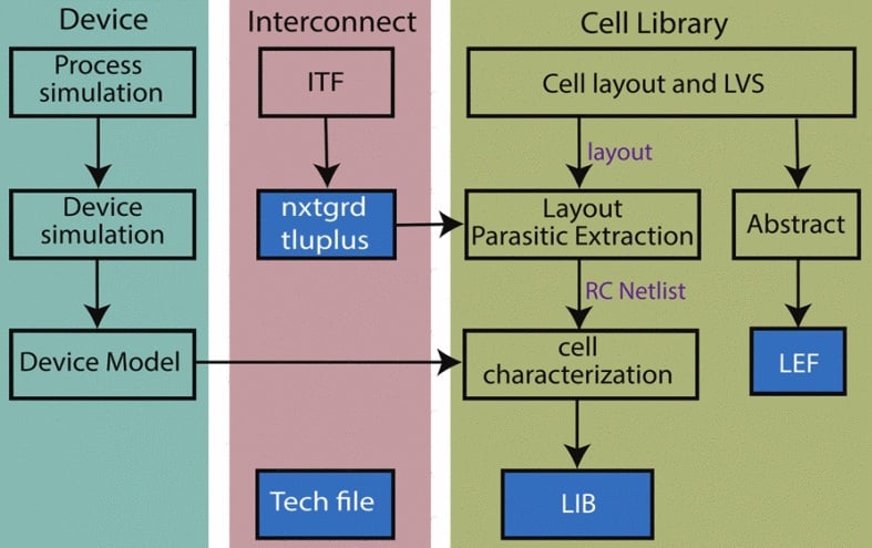
Figure 1. PDK generation flow. Image used courtesy of S. Shaji, et al.
The transistors are simulated using software tools like TCAD. The device DC and AC behaviors are captured in the transfer, output, and capacitance characteristics. A variety of BSIM (Berkeley short-channel IGFET) device models are available for this purpose.
Transistors have undergone significant changes as the technology has scaled down. Until Intel introduced the first 3D tri-gate (FinFET) transistor at the 22 nm node, the planar transistor architecture dominated the foundry business. Years later, Samsung shifted the trajectory again with the introduction of Gate All Around FET (GAAFET) architecture.
At technology nodes 22 nm and below, using multi-gate devices like FinFET and GAAFET requires BSIM-CMG templates. Each device model comprises a set of SPICE parameters whose values are extracted through curve fitting of the device characteristics. Foundries employ work function engineering to create multiple threshold voltage (Vt) options for both NMOS and PMOS transistors.
Cell Library Development
The final step is the development of a standard cell library. This must include electrical schematics for each cell that the user intends to include in the cell library. Figure 2 provides an example of a standard cell layout.
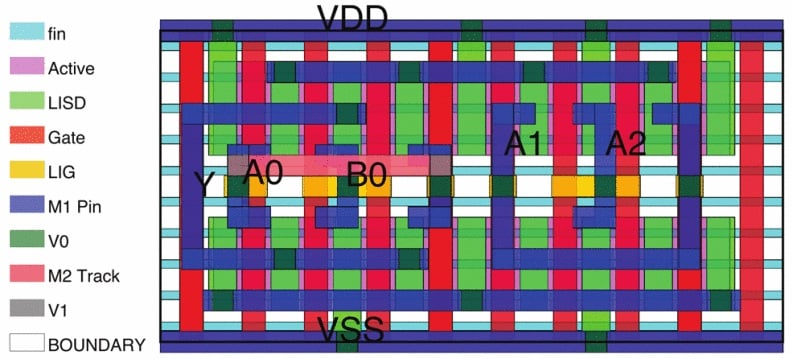
Figure 2. Cell layout for cell aoi31_x2. Image used courtesy of X. Xu, et al.
Standard cell layouts are drawn compactly, confining intra-cell routing to the lower BEOL layers (typically M1–M3) and the MOL interconnects. The cell layouts are drawn by placing the various transistors in the schematic and routing the nets. While drawing the layouts, it's crucial to carefully study the process flow, lithographic limitations, and design rules.
Once drawn, layouts need to pass a layout-versus-schematic (LVS) check. First, layout netlist extraction detects devices, contacts, and wires. The LVS tool then compares the extracted netlist with the schematic. The layout is also checked for design rule violations during the Design Rule Check (DRC) step, ensuring it can be fabricated.
Not all the information in a layout is necessary for place-and-route simulation. The shapes defining the device intricacies and internal contacts are not typically used. Instead, abstracts of the layouts are extracted into LEF files for place-and-route simulation. The LEF includes the cell boundary, pins, intra-cell interconnects on metal layers available for routing, as well as layers needed to guide the placement of the cells.
In addition to LEF files, place-and-route EDA tools also require power and timing models of each cell in the cell library. These models are generated through a two-step flow: cell parasitic extraction followed by standard cell characterization.
Parasitic extraction captures the MOL and lower BEOL layers and represents them as an RC SPICE netlist. Characterization takes these cell netlists, along with the device compact models, to generate propagation delay, transition times, and internal energy for various input slew and output load.
This information is then stored in Liberty (.lib) files. These models aid the EDA tools in estimating the design performance during block place-and-route simulation.
Wrapping Up
RTL simulation is foundational to digital IC design, and these simulations rely on accurate PDKs. In this article, we discussed the most important aspects of PDK generation for digital standard cell libraries. The key takeaways from this discussion are:
- PDK generation is a multi-stage workflow that starts with defining the BEOL metal stack, proceeds through device (FEOL) modeling, cell-level layout and verification, and finally generates the collaterals needed for place-and-route tools.
- The technology file (.tf) delivers the design rules required for a complete, manufacturable design layout.
- Accurate parasitic modelling and standard-cell characterization generate reliable timing and power models for realistic timing/power analysis.
- Standard-cell layouts are drawn to be compact, with intra-cell wiring confined to MOL and lower BEOL layers. The inter-cell routing at the block design level uses the full BEOL stack.
Featured image used courtesy of Adobe Stock