 Facebook
 Google
 GitHub
 Linkedin
Band-stop Filters
How to Create a Band-stop Filter?
Also called band-elimination, band-reject, or notch filters, this kind of filter passes all frequencies above and below a particular range set by the component values. Not surprisingly, it can be made out of a low-pass and a high-pass filter, just like the band-pass design, except that this time we connect the two filter sections in parallel with each other instead of in series.
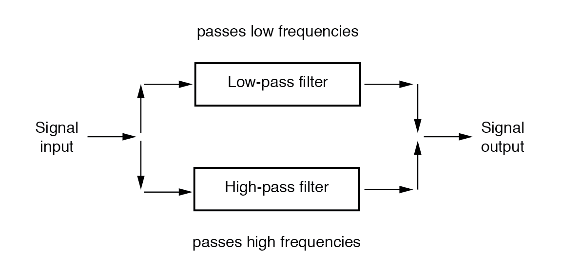
System level block diagram of a band-stop filter.
Twin-T Band-stop Filter
Constructed using two capacitive filter sections, it looks something like:
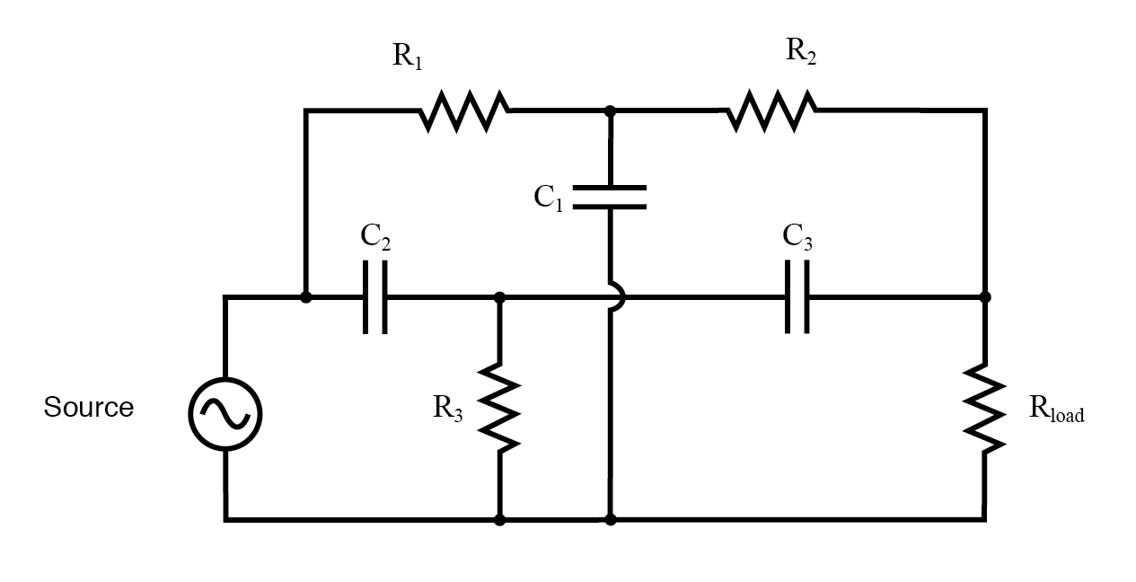
“Twin-T” band-stop filter.
The low-pass filter section is comprised of R1, R2, and C1 in a “T” configuration. The high-pass filter section is comprised of C2, C3, and R3 in a “T” configuration as well. Together, this arrangement is commonly known as a “Twin-T” filter, giving sharp response when the component values are chosen in the following ratios:

Notch Frequency
Given these component ratios, the frequency of maximum rejection (the “notch frequency”) can be calculated as follows:

The impressive band-stopping ability of this filter is illustrated by the following SPICE analysis:
twin-t bandstop filter
 v1 1 0 ac 1 sin
 r1 1 2 200
 c1 2 0 2u
 r2 2 3 200
 c2 1 4 1u
 r3 4 0 100
 c3 4 3 1u
 rload 3 0 1k
 .ac lin 20 200 1.5k
 .plot ac v(3)
 .end


Response of “twin-T” band-stop filter.
REVIEW:
- A band-stop filter works to screen out frequencies that are within a certain range, giving easy passage only to frequencies outside of that range. Also known as band-elimination, band-reject, or notch filters.
- Band-stop filters can be made by placing a low-pass filter in parallel with a high-pass filter. Commonly, both the low-pass and high-pass filter sections are of the “T” configuration, giving the name “Twin-T” to the band-stop combination.
- The frequency of maximum attenuation is called the notch frequency.
RELATED WORKSHEETS:


Can you explain the purpose of R2 and C3?