Facebook
 Google
 GitHub
 Linkedin
Introduction to Current Sources
Ever since the dawn of analog IC design (all the way back in 1962), a succession of very clever people have been trying to conjure up something that would produce an accurate current. The results have been uniformly dismal.
There happens to be a capable voltage source in ICs, the bandgap reference (which we shall get into next). So, to get a current, one would think that all one needs is an accurate resistor; after all, I = V/R. But unless you want to add a costly thin-film layer and laser trimming, there are no accurate resistors. What we get are resistors made from diffused or deposited silicon layers, which vary in resistance from wafer to wafer and have a considerable temperature coefficient.
So, don't expect any precision here. At best, an integrated current source can provide a small current without using large-value resistors and make this current more or less independent of the applied voltages.
The Quality of a Current Source
An ideal current source maintains the current level no matter what happens at its terminals, which results in an impedance that is infinite.
As we will see, a practical current source can approach this over a limited voltage range. With an impedance of up to tens of MΩ, there is very little change in current as the voltage across the current source changes. But its absolute level is subject to (absolute) parameter variations, which are large in an integrated circuit.
A Simple Current Source With a VBE Reference
The first bipolar current source example uses a diode-connected transistor (Q3) as a reference voltage (Figure 6-1). A primary current flows through R2, Q2, and Q3. The base of Q1 is at two VBE (base-emitter or diode voltage), thus, its emitter has a potential of one VBE. The output current (I1) flows through Q1 and is, thus, VBE/R1.
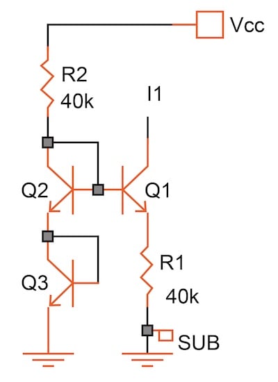
Figure 6-1. Current source based on VBE of Q3.
Output Impedance of the Simple Bipolar Current Source
If we let the voltage at the collector of Q1 drop below about 1 V, Q1 saturates and draws from the primary current. But above 1 V the output current is very constant, changing less than 0.3%, as shown in Figure 6-2.

Figure 6-2. Output current (I1) vs. collector output voltage.
This performance characteristics of the current source is best expressed as output impedance: the change in voltage (4 V) divided by the change in current (about 53 nA). Thus the output impedance of this circuit is about 75 MΩ. Not bad for using only 80 kΩs in resistance.
Non-Ideal Performance of the Simple Current Source
A diode has a negative temperature coefficient, while a diffused resistor has a positive one. The two combine to give the current a strong negative temperature coefficient, a change of about -29% from 0 to 100 °C.
In addition, the base-emitter diode is, of course, no Zener diode. The diode voltage, VBE, varies a bit as the current changes, which makes the output current, I1, dependent on the supply voltage (Figure 6-3). As the supply voltage moves from 4.5 to 5.5 V, the output current increases by 2% .
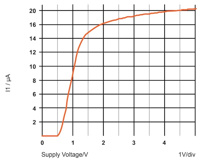
Figure 6-3. Output current (I1) vs. supply voltage.
And then there is the variation in production: ± 28%, mostly caused by the variation of R1. Changes with temperature and supply voltage must also be added to this variation.
Also, be aware that we are wasting some current: it takes 90 μA through R2 to produce 20 μA in Q1.
Important Assumptions for the Current Source Examples
Before we go on, let’s have a word about the choices in the examples of this chapter:
- Resistor variation: For bipolar circuits, the use of (base) diffused resistors is assumed with an absolute variation of ± 25%. This is probably the largest variation you will encounter; CMOS foundries often guarantee smaller variations, especially for poly resistors.
- Output current: Each current source produces about 20 μA, an arbitrary choice made to allow comparison.
- Sinks vs. sources: Strictly speaking, these circuits are current sinks, not sources. To make a circuit in which the current is delivered from the positive supply, the design is turned upside-down: NPN transistors are made PNP and N-channel ones P-channel.
- Supply voltage: These are arbitrarily selected from 5.0, 3.0, and 1.8 V.
- Fourth transistor terminal: The fourth terminal of a bipolar transistor is hidden; all of these terminals are connected together to the most negative supply voltage with the symbol SUB. This avoids cluttering up the schematic. For MOS transistors, the connection is left visible as a choice needs to be made for the P-Channel device.
An Improved Bipolar Current Source
On to the second example, a rare case where better performance is achieved with fewer devices. In Figure 6-4, Q2 regulates the current of Q1 through feedback, holding I1 more constant.
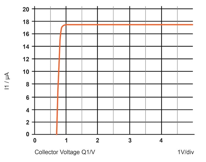
Figure 6-4. Improved VBE current source.
With this feedback regulation, the output impedance increases to 500 MΩ as shown in the Figure 6-5.
Figure 6-5. Output current (I1) vs. output voltage for the improved VBE current source.
The Monte Carlo variation decreases to ± 26%, and the change with supply voltage from 4.5 to 5.5V to +1.8% (Figure 6-6). But the voltage at the collector of Q1 still must not drop below about 1 V.