Facebook
 Google
 GitHub
 Linkedin
Low-Voltage Current Sources Using Bipolar Transistors
In our previous section, we examined two bipolar current source designs in which the emitter voltage of the output transistor is one VBE, about 0.65 V at room temperature (and higher at low temperature). For low-voltage ICs, we need a design in which this emitter is at or very near ground.
The ΔVBE Current Source
Figure 6-7 looks like a current mirror, but it isn't. There is a deliberate mismatch between the two transistors. Q1 and Q2 have the same voltage at their bases. However, while Q2 has a straightforward base-emitter diode to ground, the current path for Q1 consists of a lower diode voltage (because of the larger area using three emitters) and a resistor.
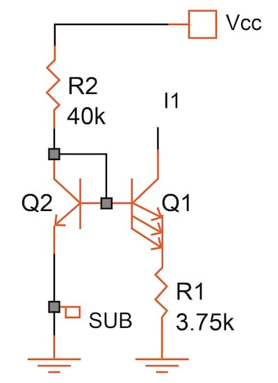
Figure 6-7. ΔVBE current source.
The difference (delta, Δ) in voltage between the two base-emitter diodes is:
$$\Delta V_{BE} = \frac {kT}{q} ln \left( \frac {A_1I_2}{A_2I_1} \right)$$
where:
k = Boltzmann constant (1.38E-23 Joules/Kelvin)
T = the absolute temperature in Kelvin
q = the electron charge (1.6E-19 Coulombs)
A1 = emitter area of Q1
A2 = emitter area of Q2
I1 = current through Q1
I2 = current through Q2
Note that ΔVBE is independent of current; only the current ratio is important. Assuming a 650 mV VBE for Q2, we can calculate the primary current (I2) as:
$$I_2 = \frac{5.0 - 0.65}{40 \text{ k}\Omega} = 109 \text{ }\mu \text{A}$$
With a desired output current, I1, of 20 μA and a 3:1 emitter ratio, we can calculate ΔVBE as follows:
$$\Delta V_{BE} = \frac {kT}{q} ln \left( \frac {A_1I_2}{A_2I_1} \right) = 0.026 \text{ } ln\left( \frac {3 \cdot 109}{1 \cdot 20} \right)= 72.6 \text{ mV}$$
Now, we can calculate the current through R1:
$$I_{R1} = \frac{\Delta V_{BE}}{R_1} = \frac{72.6 \text{ mV}}{3.75 \text{ k}\Omega} = 19.4 \text{ }\mu\text{A}$$
The voltage at the collector of Q1 can now go lower, to the saturation voltage of the device plus the ΔVBE.
There is little change in current as the voltage at the output changes (Figure 6-8). The impedance is about 12 MΩ.
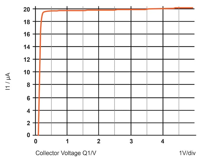
Figure 6-8. Output current (I1) vs. output voltage for the ΔVBE current source.
However, as shown in Figure 6-9, the dependence on the supply voltage is quite large, a +6.5% change as Vcc moves from 4.5 to 5.5V.
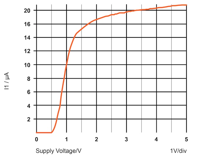
Figure 6-9. Output current (I1) vs. supply voltage for the ΔVBE current source.
Since ΔVBE is proportional to absolute temperature (PTAT), I1 has a marked positive temperature coefficient, moderated only slightly by the positive tempco of the resistors. Production variation (at a fixed voltage and temperature) is ± 26%, dominated by the variation of R1.
Improving the ΔVBE Current Source
The performance can be improved slightly by using a larger device ratio. With Q1 having 10 emitters, the output impedance increases to 15 MΩ and the voltage dependence to 4.5% (4.5 to 5.5 V).
You can also improve this performance with a simple measure. Suppose you connect the base of Q1 not to the base of Q2 but to a point that counteracts a rising Vcc. By inserting a small amount of resistance in the collector path of Q2, as shown in Figure 6-10, we get a node whose voltage is fairly constant.
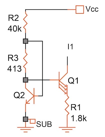
Figure 6-10. R3 reduces supply-voltage dependence.
The voltage at the base of Q2 still increases somewhat as Vcc is increased, causing its collector current to increase. But this makes the voltage drop across R3 increase, and, with just the right value, the base voltage for Q1 changes little, at least over the critical range in supply voltage.
Note that, because of the lower base voltage, the value of R1 is lower for the same amount of current. The easiest approach to circuits like Figure 6-10 is simulation. Just try various values for R1 and R3 until you get the right current with minimal change. But, in the layout, make these resistors fairly wide; you are counting on matching.
As seen in Figure 6-11, the change in I1 is now a mere ±0.5% with Vcc varying between 3.0 and 3.6 V (and even lower with a 4.5 to 5.5 V range).
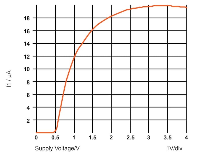
Figure 6-11. Output current (I1) vs. supply voltage with R3 optimized for the range of 3.0 to 3.6 V.
The temperature coefficient for this circuit is somewhat larger: a +31% change from 0 to 100 °C. The output impedance drops to about 7 MΩ. Production variation is unchanged.
Self-Starting Current Sources
We are about to take a rather daring step. The primary current in the previous current source circuits is a nuisance; it wastes power and requires a considerable (large) resistance. Why not replace it with a current source derived from the current the circuit generates?
There is one flaw in this argument: the current must exist first. There are two possible modes, one in which the current levels are as intended and one where there are no currents at all. In other words, there must be a current in Q2, which can be mirrored and fed back to Q1 and the base of Q2, so Q2 can have a current, etc.
The usual solution is to employ a start-up circuit designed to bring Q2 to a level sufficient to sustain the loop. The start-up circuit then shuts down and has no further influence.
But there is another way: leakage currents. In the circuit of Figure 6-12, Q2 has two leakage currents, from collector to substrate and from collector to base. These currents may be small (pA), but they are mirrored by Q3 and fed back into the base of Q2, where they are amplified. And so it goes around the loop, eventually reaching microamperes.
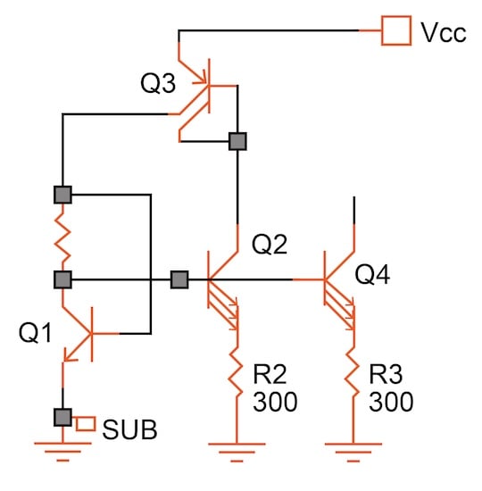
Figure 6-12. Self-starting current source without large-value resistors.
Two factors must be understood here. First, we are not talking about a leakage current caused by dirt. The very small reverse junction currents measured in today's IC devices are fundamental phenomena and have nothing to do with cleanliness.
Second, the design and the process must allow these small currents to grow. If, for example, there is a path from the base of Q3 to Vcc or the bases of either Q1 or Q2 to ground, which can shunt leakage (provided, say, by a very large, reverse-biased junction), the scheme won't work.
If your models are accurate, trust the simulation. Use a Monte Carlo analysis to see if the circuit starts up every time, and do this at temperature extremes where leakage currents are either at their lowest or highest.
R1 has been added to counteract the remaining dependence on Vcc (caused by the Early effect in Q2 and Q3). With that, we get a change of +0.4% as Vcc increases from 4.5 to 5.5V. The circuit can have a supply voltage as low as 1 V (Figure 6-13), and the voltage at the output can be as low as 0.3 V.
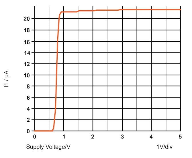
Figure 6-13. Output current (I1) vs. supply voltage for the self-starting current source.
The Erdi Current Source
Lastly, the Erdi current source of Figure 6-14 is a very clever design with an astonishing performance. We start with an auxiliary current, Iaux. And, before you even have a chance to sneer at the fact that a current source is used to make a current source, let me point out that the accuracy of this current source is of no great importance. A bulk (epi) pinch resistor or any of the lesser current sources discussed above will do.
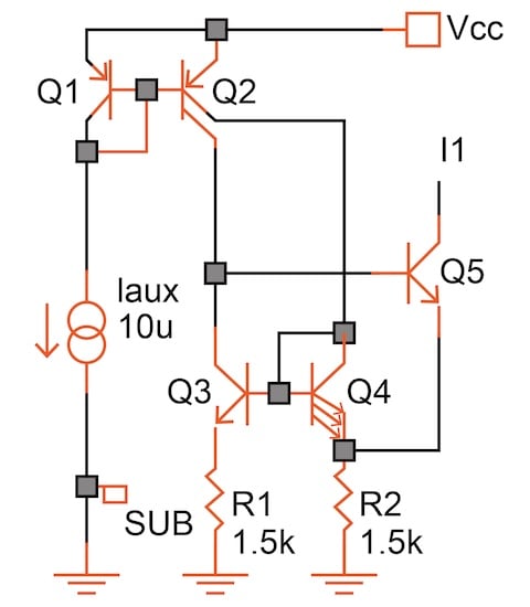
Figure 6-14. Erdi current source.
Iaux is mirrored and split into two equal parts by Q1 and Q2. Thus, the operating currents for Q3 and Q4 are equal. Q4 has three emitters and Q3 only one, thus there is a difference of about 29 mV (at room temperature). Unbalanced, the collector voltage of Q3 rises until Q5 supplies enough current to make up the difference. This current amounts to ΔVBE/R2.
Vcc can be as low as 1 V or as high as breakdown voltages allow (Figure 6-15). Moving Vcc 20% changes I1 by 0.08%. The output impedance is 50 MΩ.

Figure 6-15. Output current (I1) vs. output and supply voltage for the Erdi current source.
Temperature is strongly positive, with a +25% change from 0 to 100 oC. And the Monte Carlo variation is roughly that of R2, here assumed to be ± 25%.