Facebook
 Google
 GitHub
 Linkedin
CMOS Current Sources
None of the bipolar schemes described in the previous sections of this chapter work well for CMOS devices. They are based on VBE or ΔVBE, for which there are no MOSFET equivalents.
Trying to use circuits such as the improved ΔVBE low-voltage current sources (Figures 6-10 or 6-14) with CMOS width ratios leads to inferior circuits. Also, due to the square-law behavior of the MOSFET gate voltage, the variations are roughly double those of bipolar designs.
The MOSFET Is a Current Source
Fortunately, the CMOS transistor is a current source. If we simply apply a constant voltage (such as a reference voltage) to the MOSFET gate, as illustrated in Figure 6-16, we create a current source. We can tailor the width and length of the device to give us the desired current.
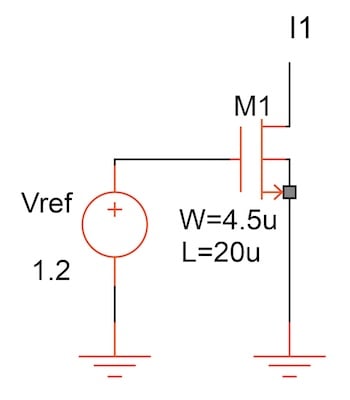
Figure 6-16. MOS transistor as a current source.
Using a rather exaggerated length, we can minimize the channel-shortening effect. In the example here, the output current varies little with the applied voltage, amounting to an impedance of 38 MΩ (Figure 6-17).
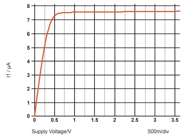
Figure 6-17. Output current (I1) vs. supply voltage for the MOS transistor current source.
However, the current variation is large and caused by a number of factors, including:
- ± 39% due to the uncertainty in the threshold voltage, VT.
- -23% variation with the change of temperature from 0 to 100oC
- A ±3% variation in the reference voltage causes a change of 10% in I1.
The ‘Ideal’ Current Source
Sometimes, a compromise is the best solution. If we allow just one component to be external to the IC and provide a pin for it, the performance of a current source improves dramatically. All other currents within the IC can then be derived from it with current mirrors and are thus inherently accurate.
In our last current source circuit of Figure 6-18, an op-amp drives the gate of the current source MOSFET M1 (or base of a bipolar transistor). The op-amp compares the voltage across the external resistor, R1, with a low internal reference voltage that could be generated by dividing down the output of a bandgap reference.
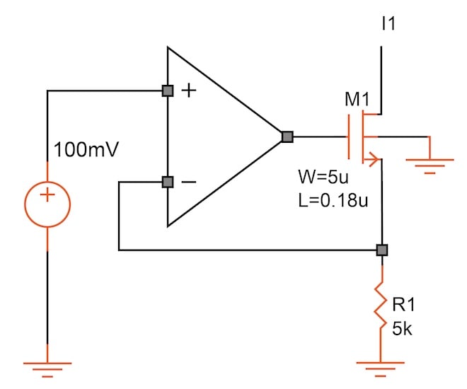
Figure 6-18. Accurate current source with an op-amp and an external resistor.
Assuming no trimming, a 1% tolerance for the external resistor, 3% for the reference voltage, and 2 mV offset uncertainty for the op-amp, I1 will be within 6% at any voltage and any temperature.