Facebook
 Google
 GitHub
 Linkedin
Simulating the Frequency Response of Amplifier Circuits
Now, let's look at a real design—the simple, bipolar op amp in Figure 8-7. I chose this rather outdated circuit because it uses the slow lateral PNP transistors, which aggravate the phase-shift problem beautifully.

Figure 8-7. An example bipolar amplifier for measuring gain and phase in a feedback loop. [click to enlarge]
The circuit uses the classical three-stage design for op amps, which we’ll discuss more in a later chapter:
- An input stage that converts the differential input signal to a single-ended one and has gain.
- A second stage (Q4) that provides more gain.
- An output stage that has no voltage gain but provides a reasonably high output current.
Since high-current PNP transistors often aren’t available in an IC, the lower portion of the output stage uses a compound transistor. From the second stage, it looks like a PNP transistor, and from the output, it looks like an NPN. The combined device is achingly slow.
Q5 and Q7 are diode-connected transistors to bias Q6 and Q8.
Simulating Amplifier Stability
The amplifier is investigated as a buffer, i.e., with a gain of one, produced by connecting the output directly to the inverting input. Here, though, there’s an inductor, L1, in the feedback path. The inductor blocks AC but lets DC through, so the circuit is properly biased.
C2 is a very large capacitor that couples an AC signal to the negative input. In this way, the feedback loop is opened up, allowing us to measure loop gain and phase. This can be done at any convenient point in the loop, but it’s clear that the most convenient is the output-to-input connection.
Note that L1 and C2 have impractically large values. This is of no great consequence since these components are for simulation only and are not going to be part of the actual design. The large values help make sure that they don't influence the AC behavior of the circuit.
As illustrated in Figure 8-7, we feed the AC signal into the loop after the inductor and then measure the loop response before the inductor (at "Out").
Amplifier Performance Without Frequency Compensation
First, let's look at the loop without the compensation capacitor, C1. The gain and phase versus frequency are plotted in Figure 8-8. They have identical scales for easier reading.
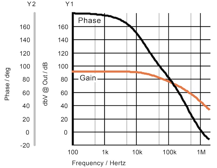
Figure 8-8. Loop gain and phase for the bipolar amplifier without the compensation capacitor C1.
The loop gain is about 92 dB, and the phase drops rather sharply, reaching zero degrees long before the gain reaches 0 dB. In fact, when the phase reaches zero degrees, the gain is still about 42 dB. Therefore, this circuit is unstable—it will oscillate.
Amplifier Performance With Frequency Compensation
In Figure 8-7, the compensation capacitor, C1, has been placed at the most strategic point in the circuit. There is considerable voltage gain between the base of Q4 and the output, which multiplies its apparent value (the Miller effect). Without this multiplication, we would need a capacitor of about 2000 pF, which is too large for an IC.
It’s also important that the capacitor feeds the AC signal from a reasonably low impedance back to a very high one. In this case, the output is fed back to the current mirror and the base of Q4. This way, we get nearly the full AC voltage swing at this point.
The result is evident in Figure 8-9. A new pole is created below 1 kHz, or about 100 times lower in frequency than the next pole.
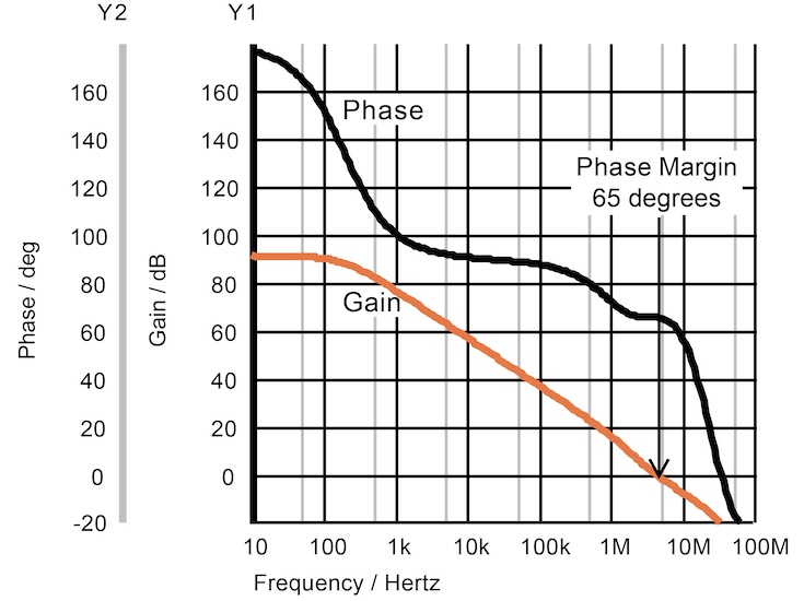
Figure 8-9. With compensation capacitor C1, the amplifier circuit has a phase margin of 65 degrees.
This pole now dominates up to at least 10 MHz, and the phase is still 65 degrees away from zero when the gain drops below one. We now have a stable circuit with an adequate safety margin.
Of course, there’s a price to be paid for this stability: the gain of the op amp may be more than 90 dB at 10 Hz, but it drops steadily as the operating frequency is increased. If we use this op amp at 10 kHz, we only have about 58 dB of gain.
Compensation for Amplifier Circuits with Gain Greater than One
This analysis has assumed that the op amp is going to be used with a gain of one. But if you are creating a design with a fixed gain, say 40 dB, there is no reason why it should have to be stable at a gain of one. This makes frequency compensation much less demanding.
Just look at Figure 8-8. Subtract 40 dB from the gain curve (only the excess gain counts), and the amplifier is almost stable, meaning that a much smaller compensation capacitor is required.
Analyzing Stability at Different DC Operating Points
The gain/phase analysis, as elegant and informative as it is, has a serious flaw: it shows performance only at one particular operating point. It is, after all, an AC analysis that does not disturb DC operating voltage and currents. A real-life signal will change the DC operating point, and the loop gain and phase can change substantially.
Some simulators let you perform this AC analysis at different DC operating points. However, there is an easier way that is a surefire test for stability:
- Get rid of the inductor L1 and capacitor C2.
- Close the feedback loop as intended in the application.
- Apply a square wave at the input. The square wave should have fast edges (the default values in the simulator are adequate).
- Then, observe the output and watch for overshoot.
For this circuit, with C1 at 20 pF, there is a slight overshoot with one peak only (see the black line in Figure 8-10). This circuit is very stable with 20 pF of compensation. You can also see that the large compensation capacitor affects the slew rate rather badly.
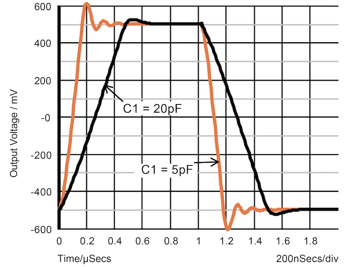
Figure 8-10. To make sure a feedback circuit does not oscillate, observe the pulse response. If there is ringing with fewer than four peaks, the circuit is stable.
With the compensation capacitor reduced to 5 pF there are three to four peaks, a damped oscillation (the orange line in Figure 8-10). Up to four peaks are acceptable. If there are more, you are asking for trouble.
To make absolutely sure, do this with a brief, 10-run Monte Carlo Analysis at the temperature extremes. Repeat this for a rapidly varying load and supply voltage; these are less likely to cause instability, but it doesn't take much time to check. If there are never more than four peaks, you are safe.
A final small hint: in a gain/phase analysis, simulators often get confused about the phase. You will see a plot that starts not at 180 degrees but at -180. The two are, in fact, the same.