Facebook
 Google
 GitHub
 Linkedin
Performance Limitations of Bipolar Transistors
There are some flaws and limitations in the performance of any bipolar transistor. These include:
- The Early effect.
- Gain as a function of current.
- Substrate current.
- Maximum voltage limits.
- Miller capacitance.
We’ll learn about all of these in due course, starting with the Early effect.
The Early Effect
The Early effect is named after Jim Early (then at Bell Labs, later at Fairchild), the first person to explain it.
Ideally, the collector current should be equal to the base current multiplied by a constant gain (hFE or beta). As we saw previously, however, each P-N junction has two depletion layers. For the collector-base junction, one depletion layer extends into the collector, and the other extends into the base.
The base is almost always more heavily doped than the collector, so its depletion layer is fairly shallow. However, the base is also very thin, so even a shallow depletion layer takes up a significant portion of the base depth.
As the collector voltage increases, the depletion layers widen. In the collector region, this has little effect as long as it doesn't hit the other side of the collector—but in the base region, it narrows the base width. Since the gain of a bipolar transistor is very much dependent on the base width, the gain simply increases as the effective base width decreases (Figure 2-17).
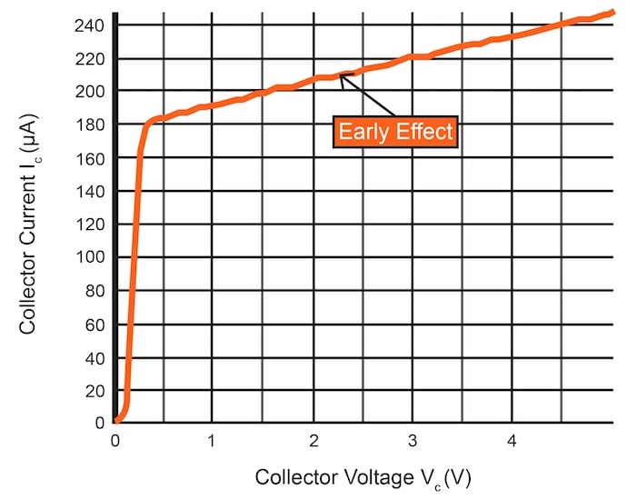
Figure 2-17. Even with a constant base current, the collector current increases with the collector-emitter voltage because the depletion layer narrows the base width.
In Figure 2-17, if you draw a straight line from 0.4 to 5 V on the I-V curve and extend the slope into the negative quadrant, it will eventually intersect with the zero-current line. This point of intersection with the x-axis is the Early voltage. For a 5 V process, the Early voltage is typically about –15 V. Generally, though, it would be expressed as 15 V. Depending on the chosen base width, it can be less than that, and the slope correspondingly steeper.
Gain As a Function of Current
For any bipolar transistor, the current gain falls off both at low and high current. Figure 2-18 plots the current gain of a bipolar transistor versus its emitter current.
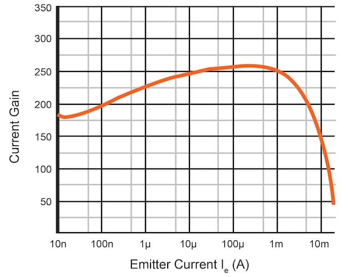
Figure 2-18. The current gain (hFE) of a bipolar transistor drops off both at low and high currents.
First, the low end. There is always a leakage current across any junction. For a perfectly clean surface, this is the diffusion current. In the base-emitter junction, this leakage current takes away a portion of the supplied base current.
In Figure 2-18, the current shunted by leakage at the low end (10 nA Ie, or about 50 pA Ib) amounts to 33% of Ib. In other words, the gain has dropped by a third. If you extend this plot to a much lower current, you’ll see the gain rise to almost infinity. This is nothing more than the effect of the collector-base leakage current.
At the high end, two effects take place simultaneously:
- The number of electrons present in the base simply becomes so large that they’re no longer the minority carriers, and the whole effect comes to a halt.
- The base current must flow from the contact to the flat area between the emitter and collector.
At low current, this is no problem because the resistance in the base is sufficiently small. But as the collector current increases—and, with it, the base current—the resistance in this flat region of the base causes a significant voltage drop. As a result, the far end gets less current.
As the current continues to increase, eventually, only the edge of the emitter on the side of the base contact is active. Thus, the high-current capability of a bipolar transistor isn’t determined by the emitter area—it’s determined by the active emitter length, which is the emitter periphery to which the base can supply current through low resistance. A good starting point for the maximum current (at which the gain drops to 50%) is 1.5 mA per µm of active emitter length, but this value varies from process to process.
Layout Techniques for Increased BJT Current Capacity
To increase the current capability of a bipolar transistor, you can place base contacts on both sides of the emitter and lengthen the emitter. Figure 2-19 shows the top views of two NPN transistors: a minimum-geometry transistor on the left and a higher-current version on the right.
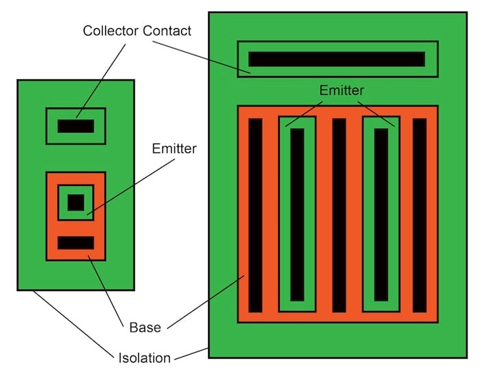
Figure 2-19. A minimum-geometry NPN transistor (left) and a higher-current design (right).
To make the life of a designer easier, the isolation pattern is usually drawn as a rectangle and then inverted when making the mask. This means that the isolation diffusion is actually between devices, not in the device area. Many processes require that all contacts be the same size, in which case the contact rectangles must be broken up into small, identical, properly spaced squares.
Be aware that transistors of different sizes, like the ones drawn here, don’t match well. At low current, a large emitter area produces a higher gain than a small one. This is because the minority carriers have a higher chance of being captured by the collector.
If you want to produce a precise ratio, use only one emitter size and identical base contacts. The emitters can be in a common base area, and the collector size is of no consequence except to the collector resistance and saturation voltage.
Substrate Current
Unless the transistor saturates, there is only leakage current across the collector-substrate junction.
Assume the collector is connected through a resistor to the positive supply voltage and the base is driven so hard that the collector voltage drops to near the potential of the emitter. This condition is known as saturation.
There are now two diodes in parallel, and the base current has two paths. The new path forms a PNP transistor as illustrated in Figure 2-20, in which:
- The NPN base becomes the emitter.
- The NPN collector becomes the base.
- The substrate becomes the collector.
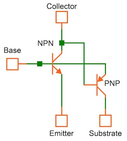
Figure 2-20. When an NPN transistor saturates, a stray PNP device leaks current to the substrate.
Since the NPN collector is much larger than its emitter, some or all of the base current flows to the substrate. There’s little danger in this, except when you drive the base very hard in an attempt to get the lowest possible collector voltage or if you have many saturating NPN transistors. The path in the substrate from a transistor to the –V connection has some resistance. If the substrate current is so large that the voltage drop across this resistance can forward-bias some substrate-collector junction on the way, you may get some really bad effects, including latch-up.
Maximum Voltage Limits of the Bipolar Transistor
To get a high operating voltage requires high resistivity and low doping concentration. But there’s a price to be paid—the depletion regions become wide.
Let's use the integrated NPN transistor as an example. There are two depletion regions:
- A depletion region extending into the epitaxial layer from the base (downward and sideways).
- A depletion region extending into the epitaxial layer from the isolation.
To make sure the first of these doesn’t reach the substrate and cause premature breakdown or punch-through, the epitaxial layer must be deep. This means that the isolation diffusion must be deep, and thus wide, as illustrated in Figure 2-21.
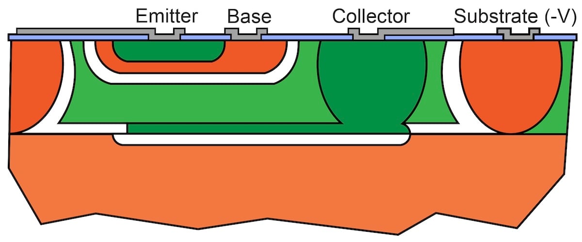
Figure 2-21. At higher operating voltages, the depletion regions around the NPN transistor become larger. [click to enlarge]
Look at the left side of the transistor. The spacing between the isolation (as drawn during layout) and the base must accommodate the following:
- The sideways diffusion of the isolation.
- The isolation-collector depletion region.
- A safety margin for possible misalignment.
- The collector-base depletion region.
- The sideways diffusion of the base.
In addition, there’s a high-voltage depletion layer between the base and the collector implant sinker, and another between the sinker and the substrate implant isolation. There is also a deeper, and thus wider, sinker. All of this adds up to a painfully large area.
The increase in area can be curbed somewhat by two measures:
- Add an additional diffusion for the isolation by creating a P+ region directly underneath the normal one before growing the epitaxial. The two halves will then diffuse toward each other (up-down diffusion) and meet in the middle, thus requiring only half the depth and width.
- Add more processing steps, creating both low-voltage and high-voltage devices on the same wafer.
The Miller Capacitance
As we saw above, the bipolar transistor is a very nonlinear (exponential) voltage amplifier. Due to its nonlinearity, it normally can’t be used as a voltage amplifier. But it does have a voltage gain, and a high one at that—several hundred is not uncommon.
There’s an unavoidable junction capacitance between the collector and the base. If you feed a current with an AC signal into the base, the voltage change on the collector will be much larger than the voltage change on the base.
When looking into the base, the junction capacitance thus appears multiplied by the voltage gain. This is the Miller effect. Instead of a tiny fraction of a picofarad, you have to deal with 10 or even 100 pF. If the base is fed from a high impedance (for example, a current source), the frequency response is then nowhere near the advertised cutoff frequency (ft, the frequency at which the current gain drops to 1).
The Miller effect can be reduced using circuit design techniques—for example, a cascode stage. Even so, most circuits cannot operate much above, say, 1/20 of ft.
On the other hand, there’s also a benefit. In feedback amplifiers, you almost always need a compensation capacitor (more on this later). Using the Miller effect, you can get away with a 5 pF capacitor, which appears to be as large as 1 nF—a value that would be much too large to be integrated.
John Miller
John M. Miller was a physicist with the National Bureau of Standards. He wrote a paper on how the grid capacitance of a vacuum tube was so much larger in use than measured statically. The paper was titled "Dependence of the input impedance of a three-electrode vacuum tube upon the load in the plate circuit" and was published in 1920 in the Scientific Papers of the Bureau of Standards. The voltage gain, he said, multiplies the capacitance between the grid and the plate. Ever since, what he described has been known as the Miller effect or Miller capacitance.
The exact same effect was found in both bipolar and MOS transistors. In most applications, it’s detrimental because it limits the frequency response. In IC op amps, however, it proved very helpful by greatly decreasing the size of the compensation capacitance.
Miller went on to do research at Atwater Kent, RCA and the Naval Research Laboratory. In 1953, he was awarded the IRE Medal of Honor.