Facebook
 Google
 GitHub
 Linkedin
Semiconductor Processing of NPN Transistors
Let's take a closer look at the basic steps in the planar process. First, you’ll need a mask—a piece of flat glass with an opaque pattern on it. The pattern is either generated optically or, more likely, with an electron beam.
The silicon wafer needs to be oxidized, meaning that a thin silicon dioxide (SiO2) layer is grown on it. This can be accomplished by exposing the wafer to steam in a furnace, among other ways. Nitride, or a combination of oxide and nitride, is also sometimes used instead of silicon dioxide.
Photoresist for Semiconductor Patterning
On top of the oxide, a thin layer of photoresist—a light-sensitive emulsion similar to that on a photograph—is spread. Light is then projected through the mask onto the wafer, as we see in Figure 2-10. The higher the frequency of the light, the greater the detail, so ultraviolet light or even X-rays are used.
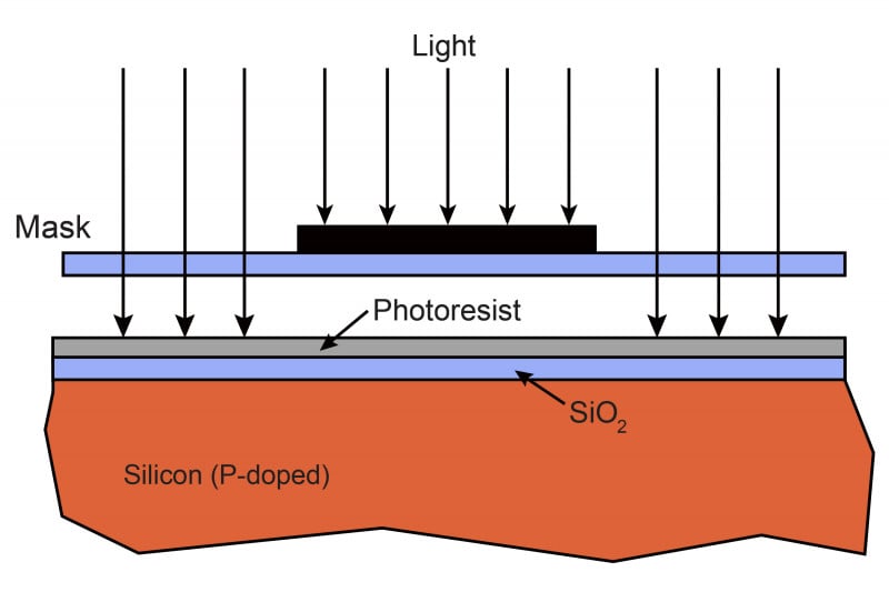
Figure 2-10. The first step: A light-sensitive and etch-resistant layer (photoresist) is spread on the wafer and exposed to light through the mask.
The photoresist is then developed, and the portions not exposed to light are washed off (Figure 2-11). Keep in mind that there are both positive and negative photoresists—you have the choice of removing either the areas that are exposed to light or the ones that are not.
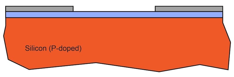
Figure 2-11. The photoresist is developed like a photograph, and the wafer is ready for etching.
Next, the entire wafer is immersed in an acid that removes the oxide in the areas where it isn’t protected by the photoresist (Figure 2-12). In more modern processes, plasma is used instead. Acid etches not only downward but also slightly sideways underneath the photoresist; plasma etches downward only.
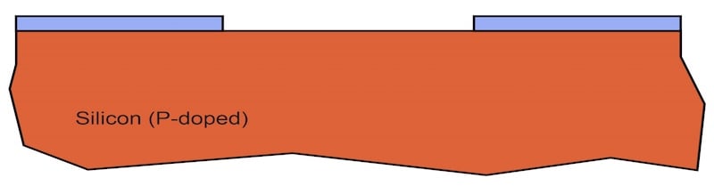
Figure 2-12. The oxide is etched away and the photoresist is removed.
Dopant Diffusion
The wafer is then placed into a furnace—a quartz tube heated to greater than 1,000 °C. A gas carrying the desired dopant (in this case, boron, arsenic, or antimony) swirls around the wafer and slowly diffuses into the surface. This can be seen in Figure 2-13.
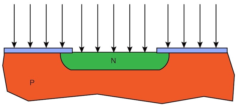
Figure 2-13. A gas containing N-type dopants (boron, arsenic, or antimony) diffuses slowly into the surface of the wafer at high temperatures.
Note two important facts here:
- Dopants crowd near the surface of the silicon. Over time, they diffuse deeper into the silicon, but there will always be more dopants near the surface. Any diffused region thus has a marked gradient.
- Dopants not only diffuse downward but also sideways. Since supply is more limited at the very edge, the sideways diffusion extends to only about half the distance of the downward one. This places the junction (the place where N = P) underneath the oxide, where it’s never exposed to the dirty environment.
After diffusion, the exposed silicon surface is covered again by an oxide layer. The wafer is now ready for the next masking step, which could be another diffusion or the etching of contact holes (Figure 2-14).
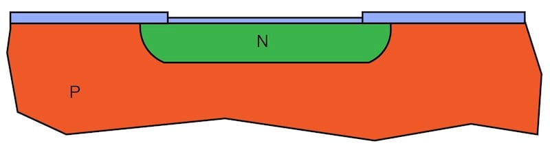
Figure 2-14. After the diffusion, the oxide is regrown, ready for the next masking step.
There’s an important feature here that shouldn’t go unnoticed. SiO2 is glass, which is transparent to light. The light is reflected at the bottom of the oxide by the silicon, creating interference patterns. In other words, the sum of direct and reflected light eliminates some frequencies. The color of the oxide layer thus depends on its thickness. This makes for beautiful photographs. More importantly, it also allows subsequent masks to be precisely aligned with previous ones.
The NPN Transistor in a Planar Process
Here, then, is one form of an NPN transistor made with the planar process. The substrate, or starting wafer, is doped P-type as the silicon is grown. There are three diffusions in succession, the first being rather deep. After the diffusions, contact holes are made using the same basic photoresist process.
Aluminum is then deposited over the entire wafer, patterned (another photoresist step), and etched away where it is not wanted. The resulting transistor is shown in Figure 2-15.
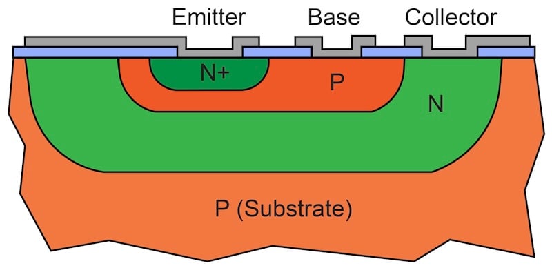
Figure 2-15. A simple planar NPN transistor.
Alas, this transistor has a rather significant shortcoming: high collector resistance. The current has to flow through the region between the base and the substrate. That’s the far end of the collector diffusion—the end that has the fewest dopant atoms and, therefore, the highest resistance.
Modern Additions to the Planar Process
New fabrication techniques have been added to the planar process since its invention.
Epitaxy
If you strip a silicon wafer of its oxide and put it into a furnace that’s filled with gas, and the gas contains not only a dopant but also silicon, you can grow a doped single-crystal layer. As the atoms carried by the gas deposit themselves on the surface of the wafer, they’ll align themselves according to the existing crystal structure.
You can also precede this by diffusing regions into the original wafer so that you’ll have areas of high concentration underneath the epitaxial layer. Even though these regions are buried, it’s still possible to align subsequent diffusions to them.
When a diffused area is re-oxidized, a small amount of silicon—the Si in SiO2—is consumed, creating a small depression in the surface. The edges of these depressions are visible at the top surface of the epitaxial layer, though the image tends to be blurry and is shifted (in most processes) about 45 degrees along the crystal axis.
Ion Implantation
You can literally shoot dopant atoms into silicon by electrically charging (ionizing) them and then accelerating them with a high voltage (several hundred thousand volts). The treatment is somewhat brutal, and the newly arrived atoms don't end up neatly aligned in the crystal structure. For the atoms to align themselves into a crystal structure, an annealing heat cycle is necessary.
The number of dopant atoms introduced is generally more accurate in ion implantation than in diffusion. You can also aim implantation for a certain depth, though not very deep. In the subsequent annealing heat cycle and diffusions, the dopant atoms will diffuse and widen the layer by doing so. Note that the maximum concentration is at a chosen depth, not at the surface.
A Modern NPN Transistor
In Figure 2-16, we’ve now arrived at a modern NPN transistor as made in a bipolar or BiCMOS (bipolar and CMOS) process. A heavily doped, buried layer of N+ ions is diffused or ion-implanted into the P-type substrate before the epitaxial layer is grown. The buried layer diffuses somewhat during epitaxy, both into the substrate and the new epitaxial layer.
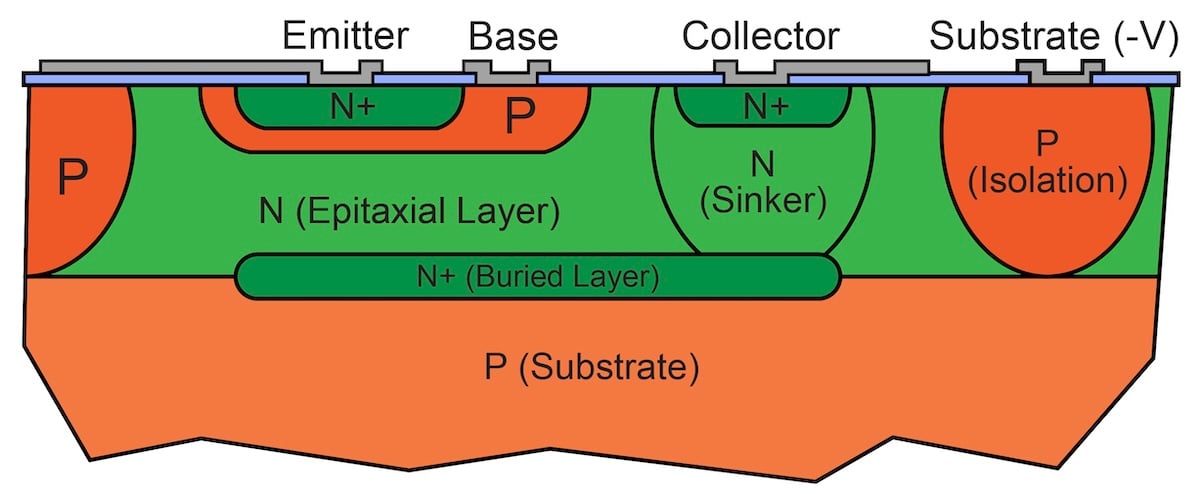
Figure 2-16. A much improved planar integrated NPN transistor. The buried layer and sinker lower the collector resistance. [click to enlarge]
The next diffusion is the isolation. The isolation is deep, and therefore also wide. It also has to connect up with the substrate so that the entire N-type collector region is surrounded by P-type regions.
A second N-type diffusion connects up with the buried layer. The emitter N+ diffusion is used on top of it, simply because it's available at no cost. Now the collector current has a fairly low-resistance path.
This transistor is isolated from its neighbors and other components as long as the substrate is held at the most negative voltage in the circuit, a state known as junction isolation. In this way, the collector-substrate junction is always reverse-biased, and only picoamperes of leakage current flow.