 Facebook
 Google
 GitHub
 Linkedin
The Diode
Even with a dopant present, silicon is uninteresting. It’s not a good conductor, and as a resistor, it’s inferior to metal film or even carbon. However, if we have both N-type and P-type atoms in the same silicon crystal, things suddenly happen.
The Diode Depletion Region
Opposite charges attract each other, so the excess electrons near the border of the N-type section move into the P-type material and stay there. An electron fills a hole, and the electric charges cancel each other out.
This only happens over a short distance, as far as an electron (or hole) can roam. The resulting region is called the space-charge layer or depletion region and is illustrated in Figure 2-4.
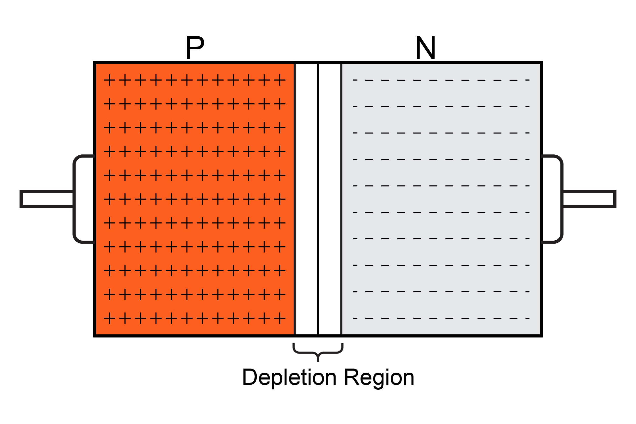
Figure 2-4. A depletion region forms between P-doped and N-doped semiconductor areas.
Now, suppose you connect a voltage to the two terminals. If the P-region is connected to the supply’s negative terminal and the N-region to the positive one, you simply push the charges away from each other, enlarging the depletion region.
If, however, the P-region is connected to the positive terminal and the N-region to the negative terminal, you push the charges closer together as the voltage increases. The closer proximity forces more electrons and holes to cross the depletion region. The effect is exponential: at 0.3 V (room temperature), very little current flows, but at 0.6 V the current is substantial, and at 0.9 V it’s very large indeed.
The Diode Current Equation
The relationship between the diode’s voltage and current is given by:
$$V_d~=~\frac{kT}{q}\text{ln}\left(\frac{I_1}{I_s}\right) $$
or
$$I_1~=~I_s \left( e^{\frac{qV_d}{kT}}~-~1\right)$$
where:
Vd = voltage across the diode
k = the Boltzmann constant (1.38E–23 joules/kelvin)
T = the absolute temperature in Kelvin
q = the electron charge (1.6E–19 Coulombs)
I1 = the actual current through the diode
Is = diffusion current
Note that 1.38E–23 is a more convenient notation for 1.38 x 10⁻²³.
Is depends on the doping level of N-type and P-type impurities, the area of the diode, and, to a very high degree, temperature. A reasonable starting point for a small-geometry IC diode is Is = 1E–16.
Breakdown Voltage
The diode current equation neglects a few things—there’s a limit to the voltage that can be applied in the reverse direction. Similar to an arc-over in any insulator, there comes a point when the electric field becomes too large, and the opposing charges crash into each other. This breakdown voltage depends on the concentration of dopants—the higher the concentration, the lower the breakdown voltage.
There’s a price to be paid for high breakdown voltage. As the dopant concentration is lowered, the depletion layer becomes larger, and the higher voltage pushes it deeper yet. This distance must be accommodated in the design.
Capacitance
The opposing charges in a semiconductor junction are no different from those on the plates of a capacitor. Every junction has a capacitance. Since the distance between the electrons and holes changes with applied voltage, the capacitance becomes voltage-dependent. The lower the voltage, the higher the capacitance, which continues increasing right into the forward direction.
Resistance and Resistivity
Lastly, there’s resistance in the semiconductor material not taken up by the depletion region. For our typical concentration of 5E–15 atoms per cubic centimeter—which gives a practical breakdown voltage in an IC of about 25 V—the resistivity is about 1 Ω·cm for phosphorus (N-type) and 3 Ω·cm for boron (P-type). Compare this to aluminum, which has a resistivity of 2.8 μΩ·cm, or copper, which has a resistivity of 1.7 μΩ·cm.
If we measure the resistance (R) across opposite surfaces of a cube, the resistivity (⍴ or rho) is given by:
$$\rho~=~\frac{R ~\times~w ~\times~ h}{l}~\rightarrow~\frac{\Omega \cdot \text{cm} \cdot \text{cm}} {\text{cm}} ~=~ \Omega \cdot \text{cm}$$
where w, h, and l are the cube’s width, height, and length, respectively.


