
 Facebook
 Google
 GitHub
 Linkedin
The CMOS Transistor
It took almost 20 years after the invention of the bipolar transistor for metal-oxide semiconductors (MOS) to make its appearance. Shockley (and many others) had thought of this device first. It should have been much simpler to build than the bipolar transistor: just put a plate close to the surface of silicon, connect it to a voltage, and move the carriers inside the silicon electrostatically.
The Troubling Silicon Surface
The problem was the surface of the silicon. Here, the silicon atoms are no longer neatly tied up with each other by sharing the outermost electrons. They face an entirely different material, silicon dioxide—or worse, some covering with unknown impurities mixed in. This material doesn't even have a crystal structure. Instead, it’s amorphous.
In 1964, a startup called General Microelectronics felt it had licked the problem with CMOS and brought out the first digital MOS integrated circuit. It was one of the worst products ever to hit the market—a large portion stopped working within days. The reason: there were elements (chiefly sodium) with the silicon dioxide that carried an electric charge and could move. One day, the MOS transistor would be perfectly functional; the next day, it would be permanently turned on.
It took another few years to gain an understanding of MOS surface physics and make stable MOS transistors. Today, the silicon surface is so well understood that we can deliberately place a charge into the oxide layer that stays there for years—probably even centuries.
CMOS Surpasses Bipolar
CMOS is now the dominant integrated device, being much smaller than the bipolar transistor. The number of MOS transistors produced every year has long surpassed the number of ants in the world. At the time of writing this book (2004), semiconductor manufacturers produced some 500 million transistors for every person in the world per year. (Editor's note: In 2024, a single integrated circuit may have more than 500 million transistors!)
The CMOS Process
Figure 2-24 shows a cross-section of the most frequently used (N-well) process. There are many variations and refinements—this is only the basic version.
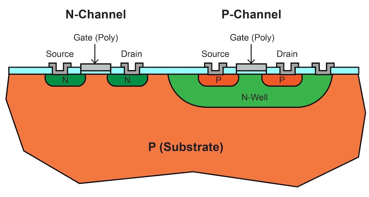
Figure 2-24. Cross-section of an N-well CMOS process. [click to enlarge]
In the gate area, the insulating layer (silicon dioxide, nitride, or a combination thereof) is thinned down and silicon is grown on top of it. Since the insulator is amorphous, the grown silicon isn’t single-crystal. Instead, we get polysilicon (sometimes simply called poly), which consists of many small crystals that don’t fit together very well.
Next, the source and drain regions are implanted using a mask. Because the inside edges are masked by the gate, they align perfectly with it. This means that they are self-aligning. The device is also self-insulating: as long as the source and drain are at or above the substrate potential (usually ground), the junctions to the substrate are reverse-biased and no bulky isolation diffusion is necessary.
For the P-channel transistor, the polarities for the source and drain implants are reversed, and these regions are placed inside an N-type diffusion. In most applications, one such N-well hosts many P-channel transistors and is directly connected to the positive supply voltage. As long as each source and drain is at or below the positive supply, the devices are insulated from each other.
In both the N-channel and P-channel transistors, sources and drains are identical—you can arbitrarily call one the source and the other the drain. Alternatively, one region can do double duty, being the drain for one transistor and the source for the next transistor connected in series.
The P-channel transistor is always at a disadvantage. Because holes are more difficult to move than electrons, a P-channel transistor will have a lower gain than an N-channel device with the same gate oxide thickness. It will also be somewhat slower.
As an aside, MOS transistors are called unipolar devices because they employ only one type of carrier, whereas both electrons and holes are important for the operation of a bipolar transistor.
Detailed Operation of an NMOS Transistor
Now let's look at an N-channel MOS transistor in more detail. The basic idea is to create a region, or channel, between the source and drain. The channel region has the same polarity as the source and drain (N-type), so that there is direct conduction between the two. This is done with a positive voltage at the gate, which pushes holes away from the surface to create the N-tyipe channel. This is illustrated at the top of Figure 2-25.
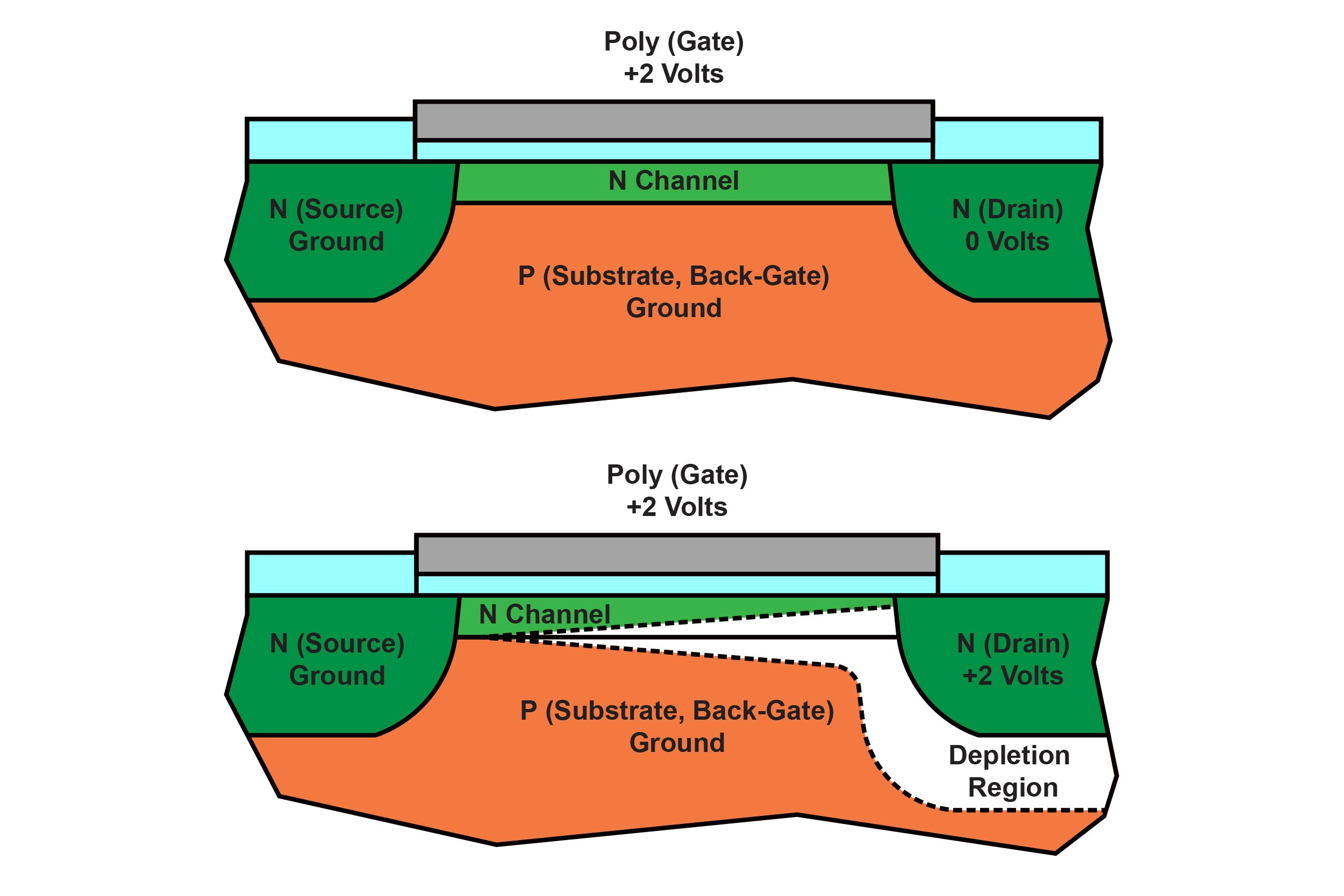
Figure 2-25. As the drain voltage is increased, a depletion region pinches off the channel. [click to enlarge]
The device is called an enhancement-mode transistor. There are also depletion-mode devices, in which a channel is implanted or diffused and then cut off with a negative gate voltage.
The channel is uniform only at zero or very low drain voltage. As the drain voltage is increased, a depletion region forms around it. This is what’s shown in the bottom of Figure 2-25. Since there’s now a voltage drop along the channel, with the drain side at a higher voltage than the source, the depletion region along the channel gradually increases toward the drain, cutting more and more into the channel. Thus, the resistance of the channel increases.
Figure 2-26 plots the drain current versus the drain voltage for an NMOS transistor.
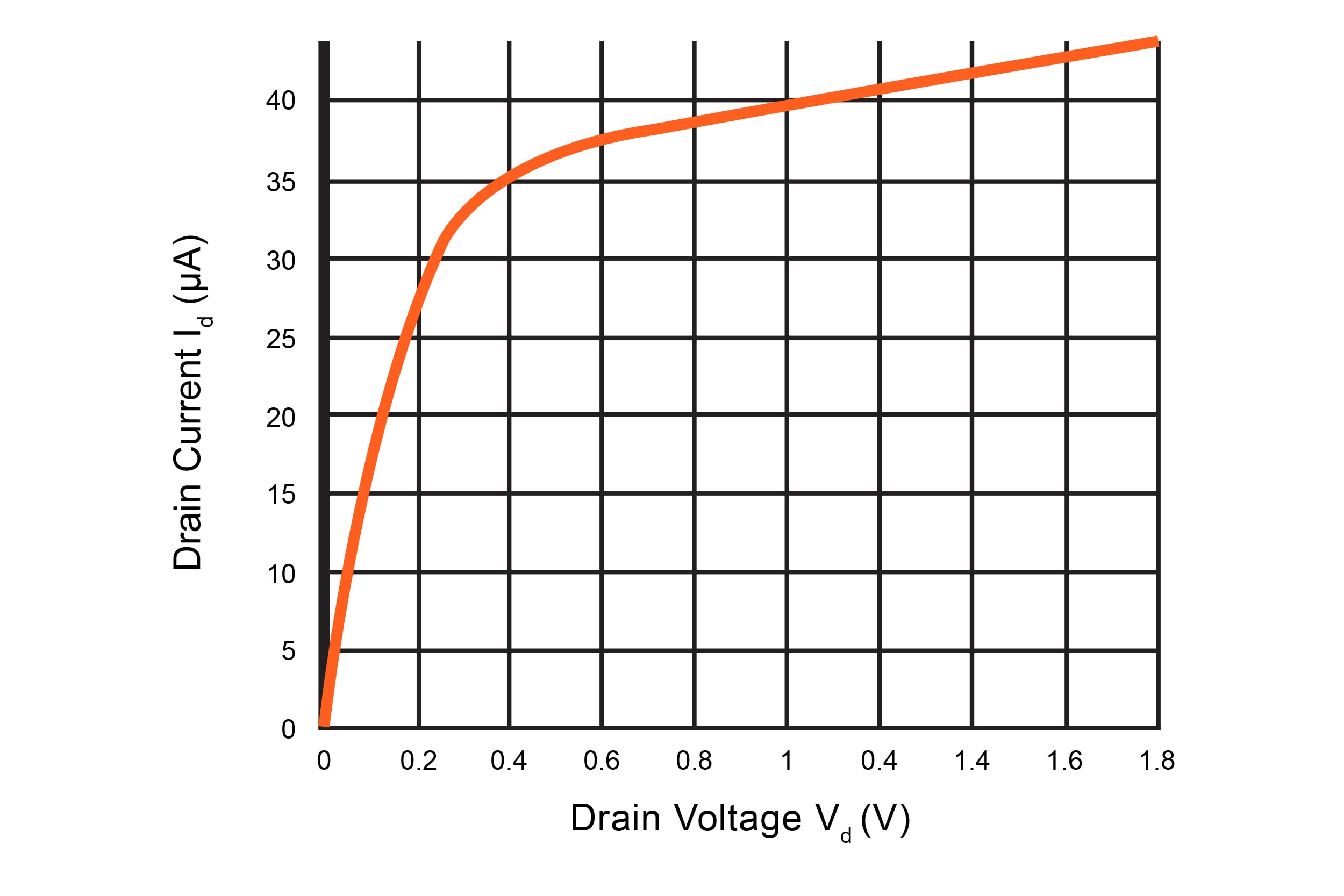
Figure 2-26. Drain current vs. drain voltage, with the gate voltage held constant.
The initial slope of the drain voltage/drain current curve is the resistance of the channel without any depletion layers. The final slope at the highest drain voltage represents its resistance with the depletion layer almost pinching off the channel. It is an unfortunate fact that this region is called the saturation region, which clashes badly with the earlier definition used for the bipolar transistor.
A certain gate potential has to be exceeded to attract any carriers to the surface. This is known as the threshold voltage. Above it, an MOS transistor is basically a square-law device. As we can see in Figure 2-27, doubling the gate voltage results in four times the drain current.
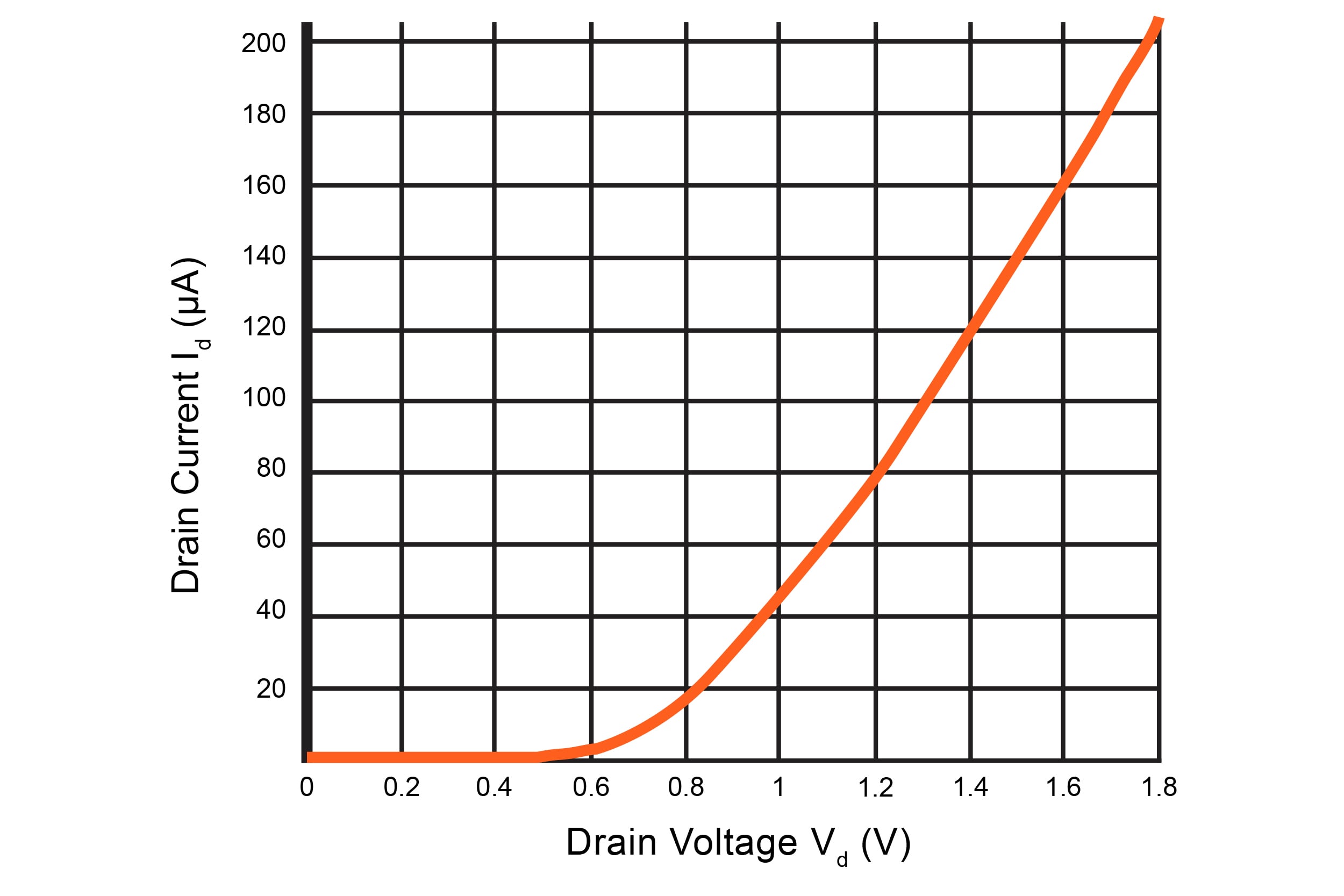
Figure 2-27. Drain current vs. gate voltage, with the drain voltage held constant.
The measure of gain is the transconductance, which is the drain current divided by gate voltage. Like the bipolar transistor, this is a nonlinear device:
$$I_{d}~=~k \frac{W}{L}(V_{gs}~-~V_{T})^{2}$$
where:
Id = drain current
k = transconductance
W = channel width
L = channel length
Vgs = gate-to-source voltage
VT = threshold voltage
Vgs – VT = gate voltage above the threshold.
The region below the channel also influences the gain. It forms a back gate. For an N-channel transistor, this is the P-doped substrate, which is common to all devices. You have no choice but to connect it to the lowest negative voltage.
There is a choice for the P-channel transistor, though. If you place all of the P-channel transistors in a common N-well, you get the smallest total area and therefore the lowest cost. But if the source of such a transistor is operated below the positive supply, the back gate (the N-well) pinches off the channel further, and you get a gain that’s reduced by perhaps 30%. You can avoid this by placing this transistor in its own N-well.
The Substrate PNP Transistor
In either a bipolar or CMOS process, there exist layers that can form a PNP transistor with the substrate as the collector (Figure 2-28).
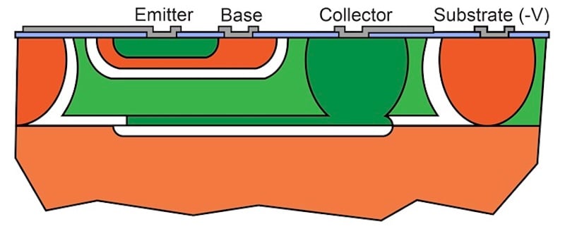
Figure 2-28. The base, collector, and substrate form a vertical PNP transistor.
Since the collector is permanently connected to the most negative supply voltage, such a device has limited use. In a bipolar process, a lateral PNP transistor has greater flexibility and better performance and is thus almost always preferred.
The same is true in a CMOS process, but—whether because of historical reasons or limited information—the substrate transistor is still present. The P-type implant for the P-channel transistor forms the emitter, the N-well the base, and the substrate the collector. The N-well has a large depth, so the PNP base width is large and the gain rather small (perhaps 10).


