Facebook
 Google
 GitHub
 Linkedin
Resistors in IC Processes
Every free-floating layer in an integrated circuit can, when properly patterned, become a resistor. This is only a secondary duty of the patterned layers—their primary application is in creating a transistor. It’s harder to create a transistor than a resistor, so it shouldn't come as a surprise that the resistor values have a higher variation and greater temperature coefficient. Their range is also more restricted than that of even the least expensive discrete resistor.
Discrete resistors can be tested and adjusted during manufacturing. In ICs, the manufacturing is done while the silicon is red-hot. At that temperature, the silicon is no longer a semiconductor—you have to wait until it cools down to measure any parameters.
What saves the integrated resistor is its natural ability to match well. Whatever error may have occurred in making one applies to any other on the same wafer. They may both be as much as 25% higher than the target value, but both will be high by (almost) exactly the same amount.
Sheet Resistance
The resistance of any material is given by:
$$R=\frac{\rho~\times~{l}}{A}$$
where:
rho (⍴) = resistivity in Ω·cm
l = length
A = area (cross-section).
If we make a square (w = l), we get a measure of resistance that is independent of size—the sheet resistance. This is measured in Ω/⃞ (ohms-per-square). Note that the term is sheet resistance, not sheet resistivity. A square in a layer with a sheet resistance of 100 Ω/⃞ always measures 100 Ω from one side to the other, no matter how large the square.
Resistor Options by Process
In a bipolar process, the layer most often used for resistors is the NPN base (about 200 Ω/⃞). The emitter layer is more heavily doped and thus has a lower sheet resistance (as low as 5 Ω/⃞).
In a CMOS process, you have a wider range of choices: the N+ and P+ diffusions (implants) for the drains and sources, the N-well, and usually two different poly layers as well. Of these, the P+ diffusion (about 150 Ω/⃞) and one of the poly layers (around 50 Ω/⃞) are generally best suited.
Sheet resistances depend greatly on the process. You should use the values given here only as a starting point and get the actual data—including temperature coefficients and tolerances—from the wafer fab.
Diffused resistors must be placed in an island of opposite doping. The island needs to be connected to a bias voltage so that the junction is reverse-biased.
For example, a P-type base resistor must be in an N-type (epi) island. This island, sometimes called the “tub,” can contain anywhere from one resistor to all of them, but its voltage must be equal to or greater than the largest voltage on any resistor. In the case of the “tub,” the easiest and safest connection is to +V.
Voltage Coefficient of Resistance
Diffused resistors—and, to a lesser degree, poly resistors—have a voltage coefficient. The biased surrounding layer pushes a depletion region into the resistor, reducing its cross-section. As the difference in voltage between the resistor and the surrounding layer becomes larger, the depletion region widens, the cross-section becomes smaller, and the resistance increases. This effect is especially pronounced in lightly doped layers—the N-well in CMOS and the implanted resistors in a bipolar process. The latter use an additional implant to create a high sheet resistance.
This voltage dependence is especially critical if you have two or more resistors that need to match but are at different DC levels. You can either:
- Place each resistor in a separate island, biased at the positive end of its resistor.
- Simply accept the change caused by the depletion layer and adjust the ratio.
For the second option, however, you need a model for the resistor that includes its voltage dependence. In a 200 Ω/⃞ base layer, for example, the change in resistance is about 1% for a 5 V bias difference.
Capacitance of Semiconductor Resistors
There’s also a distributed capacitance associated with an integrated resistor. It’s low for poly resistors, but higher—and voltage dependent—for diffused ones. If you make a very long resistor with a high-value resistance, this stray capacitance can seriously cut frequency response. Also, if there’s noise on the supply that biases the surrounding region for diffused resistors, it will be capacitively coupled into the resistor. Again, a good model is required to show these effects in a simulation.
Resistor Correction Factors
Two correction factors must be used when designing a resistor. The first concerns the width of the resistor. In diffused or implanted resistors, there is always a sideways diffusion. This makes the actual resistor wider than drawn. The effect of the sideways diffusion is dependent on the width of the resistor.
The second correction factor recognizes the end-effect. If the resistor is of minimum width, you’ll need to enlarge both ends to place a contact inside. This is illustrated at the top of Figure 2-30. You’ll then need to estimate the resistance of this additional area (totaling perhaps 0.4 squares from the end of the narrow part) and of the contact itself.
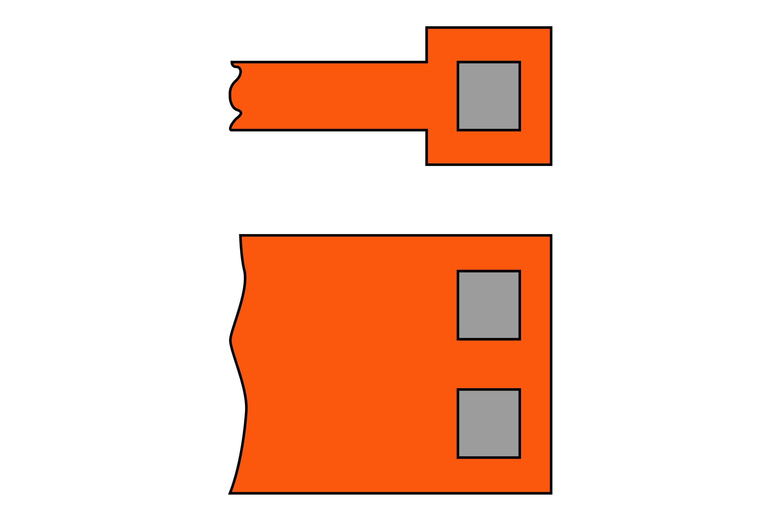
Figure 2-30. Resistor contacts for a minimum-width resistor (top) and a wide resistor (bottom).
If you draw a wide resistor, the contacts can be fitted inside it. This is shown at the bottom of Figure 2-30. However, they won’t cover the entire width even if converted to one long contact. There is, therefore, a small (about 0.2 squares from the inside edge of the contacts) additional resistance.
The matching of resistors depends entirely on width. Submicron processes aren’t designed for good matching, just maximum speed. You’ll find that minimum-dimension devices—all devices, not just resistors—match very poorly.
When greatly magnified under a microscope, all edges appear somewhat ragged. The width of a resistor, for example, fluctuates considerably. It’s only when you make a relatively large device that these fluctuations become insignificant, and the device matches well. Figure on using something like ten times the minimum width to get a matching of 0.5% or better.
Because of the end-effect, you can’t expect resistors of different lengths to match well. For optimum matching, use only identical resistors. It also helps to divide resistors into identical sections and intermingle them with other resistors in the same identical sections that are intended to match.
The Seebeck Effect
Before we move on to the next type of resistor, we have one more thing to discuss: the Seebeck effect. In 1821, Thomas Seebeck discovered that metallic interfaces at the ends of a wire produce a voltage if the ends are at different temperatures. Four years later, Georg Ohm used this effect to measure resistance. Today, it’s used in thermocouples.
For the contacts of a diffused or poly resistor, the Seebeck voltage is between 0.2 mV/°C and 1.4 mV/°C, depending on the doping level and composition of the metal. This is a danger if thermal gradients are present—for example if there is a power transistor on the chip. To avoid the danger, lay the resistor out so that its beginning and end are close together.
Pinch Resistors
Pinch resistors (or pinched resistors) are sometimes used in bipolar processes to get a high resistance without wasting a lot of area. Figure 2-31 shows a base-pinch resistor, which is simply a base resistor with the emitter diffusion placed over part of it. This placement reduces the effective cross-section—only the deepest part of the base diffusion, which also has the highest resistance, is left. The device needs to be in its own epi island, with the epi and the emitter diffusion connected to the positive terminal.
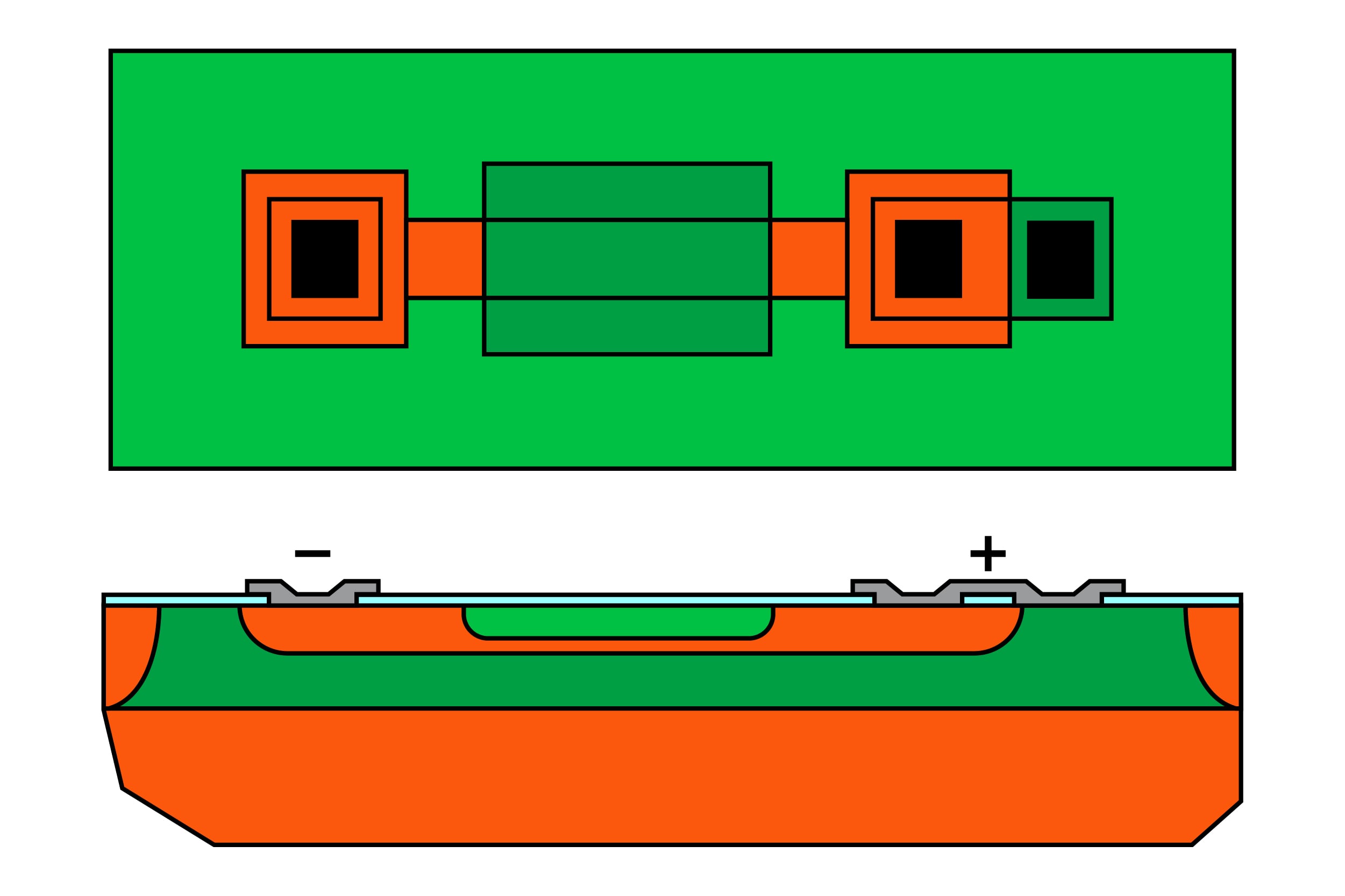
Figure 2-31. Top view and cross-section of base-pinch resistor. [click to enlarge]
A base-pinch resistor is nonlinear. It has a low (perhaps 6 V) breakdown and a large (about 10:1) variation. However, you can cram 100 kΩ of resistance into the space of a transistor.
Next, let's examine the epi-pinch resistor (Figure 2-32).
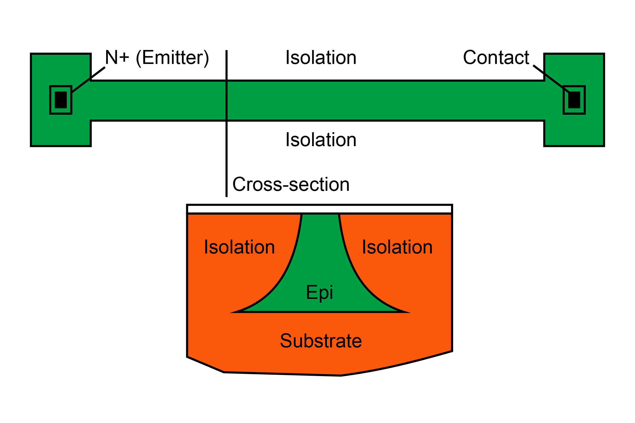
Figure 2-32. Top view and cross-section of epi-pinch resistor. [click to enlarge]
In the epi-pinch resistor, the cross-section of a long and narrow epi region is further reduced by moving the isolation diffusions on either side very close together. The epi region is usually of fairly high resistivity. As a result, a substantial depletion region extends into the remaining epi region, pinching it off at an operating voltage that’s above the substrate potential and in excess of about 5 V.
At any voltage higher than that, the epi-pinch resistor becomes a current source. The variation of this current is high (8:1), but you can create a small current of a few μA in relatively little space.