Facebook
 Google
 GitHub
 Linkedin
Diodes in Semiconductor Processes
There are several P-N junctions in an integrated circuit, each and every one of which is a diode. Few of them, however, can actually be used by themselves without unpleasant side effects.
For example, take a simple bipolar process. There are three types of junctions. In an NPN transistor, these are:
- Emitter-base.
- Base-collector.
- Collector-substrate.
The last one is hardly ever useful because the substrate is permanently connected to the most negative supply voltage. The base-collector diode is, as we’ve already seen, part of a substrate PNP transistor with a gain. A current, perhaps ten times the magnitude of the diode current, will flow to the substrate.
The emitter-base junction makes a good diode, but it has a low breakdown voltage (about 6 V), and the base has a fairly high resistance. You could connect the surrounding collector to the most negative supply voltage, which would keep it perpetually reverse-biased. However, a much better diode results if you short the collector and base together to create a diode-connected transistor like the one in Figure 2-29.
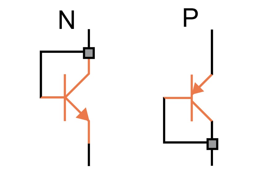
Figure 2-29. Properly connected diodes in a bipolar process.
The diode-connected transistor is active—it has gain. Only a small fraction of the current flows through the base, which divides the base resistance by the current gain. In fact, this connection gives you an almost ideal diode over about five decades of current.
If the emitter-base breakdown voltage is too low, consider a diode-connected lateral PNP transistor. This device has the full operating voltage of the process. However, as we learned earlier in this chapter, it’s limited in current.
In a CMOS process, the restrictions are even more severe. The only free-floating junction is between the P-channel source-drain and the N-well. As we’ve seen, however, these are also part of the substrate PNP transistor. Were you to run a current through this junction, a current of about ten times its magnitude would flow to the substrate.
As an aside, the term "diode-connected" is often used for an MOS transistor with its gate and drain connected together. Don't be misled by this term—there’s no diode in the sense of a junction diode.
Zener Diodes
In a bipolar process, the base-emitter diode almost always has a low breakdown voltage with a fairly low temperature coefficient. This makes it useful as a reference voltage. But exercise care with this device—the same junction is also used as a fusible device.
At low current (less than 100 µA for a minimum-geometry device), the Zener diode behaves well. As you increase the current, the region between the emitter contact and the edge of the emitter diffusion lights up faintly—it’s a plasma, which you can observe under a microscope with all the lights turned off.
At some high current level, a thin aluminum strip forms abruptly underneath the oxide, converting the Zener diode into a short-circuit. This effect, which is used for trimming, carries the earthy name Zener-zapping.
Such a Zener diode is also somewhat noisy. For lower noise and better accuracy, use a bandgap reference. Moving an N-channel and P-channel source/drain diffusion in a CMOS process close together so that they intersect can also result in a usefully low breakdown voltage, but data for such a device is rarely available from the wafer-fab.
There are also buried Zener diodes, devices with a special diffusion below the surface of the wafer. These devices have lower noise, but their addition to the process tends to be costly.