Facebook
 Google
 GitHub
 Linkedin
The Semiconductor Industry and the Planar Process
When, in 1956, the three inventors of the transistor were awarded the Nobel Prize for physics, only Walter Brattain was still at Bell Laboratories. John Bardeen left in 1951 to become a professor at the University of Illinois. For his research there in superconductivity, he received a second Nobel Prize in 1972.
The Birth of the Semiconductor Industry: Shockley Semiconductor
Bill Shockley left Bell Labs in 1954. Banking on his reputation, which had risen proportionally to the acceptance of the transistor, he managed to strike a deal with the Beckman Instruments Company. A subsidiary called the Shockley Semiconductor Laboratories was set up in Palo Alto, California.
Shockley's fame had risen to such a height that he could pick some of the best people. Within a year, he had some 20 people—predominantly PhDs—working for him. Among these were Robert Noyce, 28, Gordon Moore, 27, and Jean Hoerni, 32.
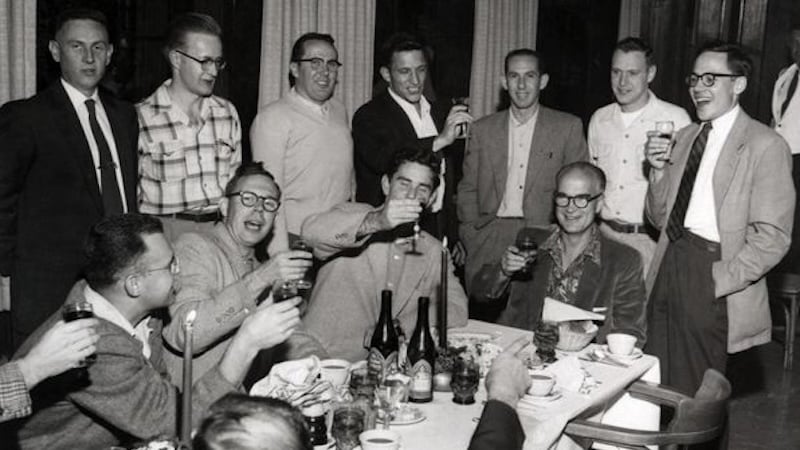
William Shockley and friends celebrate the Nobel Prize announcement. Image used courtesy of the Computer History Museum
For all of these people, there was a brief period of fascination after they joined. But then the true Bill Shockley appeared from behind the glitter of fame, and they discovered that Shockley was, in fact, a rather erratic and unpleasant man. He would fire his employees for minor mistakes, throw tantrums over trivial problems, and change directions for no apparent reason. He incessantly tried innovative management techniques—posting everybody's salaries on the bulletin board, for example.
Noyce and Moore were pushing Shockley to make silicon transistors using the diffusion approach. Shockley wasn't interested—his hope was for his laboratory to come up with an entirely new device, a device that would represent as large a step over the transistor as the transistor had been over the vacuum tube.
Now totally dissatisfied, the crew talked to Arnold Beckman, the president of the parent company, and informed him of the impossible situation. Beckman promised to hire a business-minded individual who could act as a buffer between Shockley and his staff. But the solution didn't work. Shockley refused to let go of the day-to-day decision-making.
Fairchild Semiconductor
Out of patience, eight staff members reached a deal with the Fairchild Camera and Instrument Company. In October 1957, the group departed. They would later be dubbed the “Traitorous Eight” by Shockley. Their new company, called Fairchild Semiconductor, was at first an independent operation with Fairchild Camera and Instrument holding an option for a buy-out.
The product they began to develop was the one they had proposed to Shockley. The detailed structure of this device—which was called the mesa transistor—had been tried in germanium before, but not in silicon. It required two diffusions, both into the same side of a silicon wafer. The first diffusion was P-type, the second N-type.
The difference in depth between the two layers created the base region, which for the first time could be made with a high degree of accuracy. The top surface of the transistor was then masked with wax and the exposed silicon etched away, giving the remaining piece a mesa-like shape.
Because of its superior performance, sales of the mesa transistor took off almost immediately, reaching $7 million in 1959. But there were also problems. The most serious one concerned the reliability of the mesa transistor. The etched silicon chip was soldered onto the bottom of a small metal case, leads were attached to the top regions, and then the case was welded shut. Tiny metal particles, ejected during the welding process, floated around inside the case and kept on shorting out the exposed P-N junctions.
The Planar Process for Semiconductor Manufacturing
Silicon rapidly grows a thin oxide layer when exposed to air. The growth of this silicon dioxide (better known as glass) can be enhanced by moisture at high temperatures. Some of the dopant gases used in diffusion—such as gallium—can penetrate this oxide layer, while others are stopped by it.
This raised the possibility of using the oxide layer as a mask. If the oxide were etched off in some places but not in others, and suitable dopant gases were used, diffusion would take place only in the areas without oxide. However, a study done at Bell Laboratories came to the conclusion that an oxide layer exposed to a diffusion is left contaminated and must subsequently be replaced by a freshly grown one.
This bothered Hoerni. He didn't see any reason why the oxide layer couldn’t be used as a diffusion mask for both diffusions, provided he used dopant gases that were stopped by the oxide, or why the oxide should subsequently be regarded as contaminated. So he tried it as an unofficial side project—and out of the trial came the planar process, an advance ranking in importance second only to the transistor itself.
In preparation for the first diffusion, Hoerni spread a photosensitive and etch-resistant coating (photoresist) over the top of the oxide and exposed it through a photographic plate (mask) carrying the patterns of the base regions, using the photographic techniques already developed for "printed" circuits. The subsequent etching only removed the oxide in the regions where P-type impurities were to be diffused.
After the diffusion, he closed these oxide "windows" again by placing the wafer in high-temperature moisture, then repeated the steps for the second (emitter) diffusion. In a third masking step, windows could then be etched in the oxide to make contact with the two diffused layers. Next, he evaporated aluminum onto the top surface of the wafer and patterned it with the same photographic techniques. The wafer could then be scribed like glass and broken into individual transistor chips.
Advantages of Planar Processing
The planar process had a whole series of advantages. Most immediately important was the fact that the junction was automatically protected by the oxide, one of the best insulators known. No longer could the metal particles from the welding of the case short it out.
Secondly, photographic methods could be used to delineate not just one but hundreds of transistors simultaneously. Individual, delicate masking of each transistor was thus no longer required, giving the planar transistor a huge potential for reduced cost. Noyce, who was by now the general manager, saw the advantage of the planar process and quietly moved it into production.
There was another advantage to the planar transistor: once the dopant enters the silicon, it diffuses in all directions, including sideways. The P-N junction therefore ends up underneath the oxide, never exposed to either human handling or the contamination of air. For this reason, the planar junction is the cleanest, most stable junction ever produced. Fairchild's customers, who in early 1959 didn't know that their transistors were now being manufactured by an entirely new process, were surprised to find leakage currents 1,000 times smaller than those of previous shipments.
While Fairchild flourished, Shockley Semiconductor went downhill. It was sold twice, then closed in 1969. Shockley became interested in sociology and announced a theory called "dysgenics," which proposed that poor people were doomed to have low IQs. By the time he died in 1989, his reputation was ruined.