Facebook
 Google
 GitHub
 Linkedin
The Birth of the Bipolar Junction Transistor
At the time of the first serious work on the semiconductor diode, Bell Laboratories in New Jersey was already world-famous. It attracted the brightest scientists, and even among those, Bill Shockley was a stand-out. In 1938, William Shockley teamed up with Walter Brattain to investigate semiconductors.
The depletion layer intrigued Shockley. There was a faint similarity to the vacuum diode. It occurred to Shockley that, if he could somehow insert a grid into this region, it might be possible to control the amount of current flowing in a copper-oxide rectifier, creating the solid-state equivalent of the vacuum triode.
Shockley went to Brattain with the idea. Brattain was amused: the same idea had occurred to him, too. He had even calculated the dimensions for such a grid, which turned out to be impractically small. Shockley tried it anyway and couldn't make it work. Brattain had been right.
Shockley was not a man easily defeated, though. He modified his idea and came up with a different principle of operation. Since a relatively small number of electrons or holes are responsible for conduction in semiconductors, and they each carry a charge, he conceived of placing a metal electrode near the surface and connecting it to a voltage, thus either pulling these carriers toward the surface or pushing them away from it.
By doing so, he thought that the conduction of the region nearest the surface could be altered at will. He tried it—and it didn't work either. The idea was identical to today's MOS transistor.
The work stopped there—both Shockley and Brattain were assigned to other projects during the war. In 1945, however, Shockley was made co-supervisor of a solid-state physics group that included Brattain. Shockley was 35 years old; Brattain was 43.
The progress made in refining silicon and germanium was not lost on Shockley, and he decided to try his idea for an amplifying device again. This time, he had a thin film of silicon deposited and topped with an insulated control electrode. It still didn't work—no matter what voltage was applied to the control electrode, there was no discernible change in current through the silicon film.
Shockley was puzzled: according to his calculations, there should have been a large change. But the effect, if there was any, was at least 1,500 times smaller than theoretically predicted.
Bardeen, Brattain, and the Point Contact Transistor
It was at this time that John Bardeen, 37, joined Shockley's group. He looked at Shockley's failed experiment and mulled it over in his head for a few months. In March 1946, he came up with an explanation: it was the surface of the silicon that killed the effect.
Where the silicon stops, the four valence electrons are no longer neatly tied up by the neighboring atoms. Bardeen correctly perceived that some of them were left dangling and thus produced a surface charge (or voltage) that blocked any voltage applied to an external control electrode.
With this theoretical breakthrough, the group now decided to change directions. Instead of attempting to make a device, they investigated the fundamentals of semiconductor surfaces. It was a long, painstaking investigation that took more than a year.
On November 17, 1947, Robert B. Gibney—another member of the group and a physical chemist—suggested using an electrolyte to counteract the surface charge. On November 20, he and Brattain wrote a patent disclosure for an amplifying device like the one tried by Shockley but using an electrolyte on the surface. Then they went to the lab and made one. The electrolyte was extracted from an electrolytic capacitor with a hammer and nail.
The device worked—the electrolyte did precisely the job that Gibney thought it would. But though this "field effect" device functioned as an amplifier, it was very slow. It amplified nothing faster than about 8 Hz. Brattain and Bardeen suspected that it was the electrolyte that slowed down the device, so on December 16, 1947, they tried a different approach.
A gold spot with a small hole in the center was evaporated onto germanium, on top of the insulating oxide. The idea was to place a sharp point-contact in the center without touching the gold ring, so that the point would make contact with the germanium while the insulated gold ring shielded the surface. By doing so, they attained amplification.
There was only one thing wrong with this device: it didn't work as expected. A positive voltage at the control terminal increased the current through the device. According to their theory, it should have decreased it.
When Bardeen and Brattain investigated, they found that they had inadvertently washed off the oxide before evaporating the gold. The gold was, therefore, in contact with the germanium. What they were observing was an entirely different effect—an injection of carriers by the point contact.
To make such a device efficient, they realized, the distance between the two contacts at the surface needed to be very small. They evaporated a new gold spot, split it in half with a razor blade, and placed two point-contacts on top. Now the device worked even better.
They demonstrated it to the Bell management on December 23, 1947. For half a year after that, Bell kept the breakthrough a secret. Bardeen and Brattain published a paper on June 25, 1948, and a press conference was held in New York on June 30. The announcement made little impression—the New York Times devoted a few lines to it on page 46.
Since he hadn’t been part of the final breakthrough, Shockley was disappointed by the turn of events. But he realized that the battle wasn't over yet—even though there was a working device, no one within the group really understood precisely how the transistor worked.
So, in the early days of January 1948, Shockley sat down and tried to figure out what was going on between the two point contacts. In the process, he conceived a much better structure: the junction transistor. It was a brilliant analysis that holds up to this day.
The Big Breakthrough
In a bipolar transistor, a current flows between the base and emitter terminals, which form a diode. Electrons flow from the emitter to the base (so named because, in the original point-contact transistor, it was the bulk of the material). Since the base is P-doped, these electrons are the minority carriers in the base. This is where we get the name bipolar transistor—carriers of both polarities are needed for the effect to occur.
A few of these electrons will reach the base terminal. However, if the base is lightly doped and very thin, most of them will be attracted by the positive collector voltage before they recombine with a hole in the base. This is illustrated in Figure 2-5.
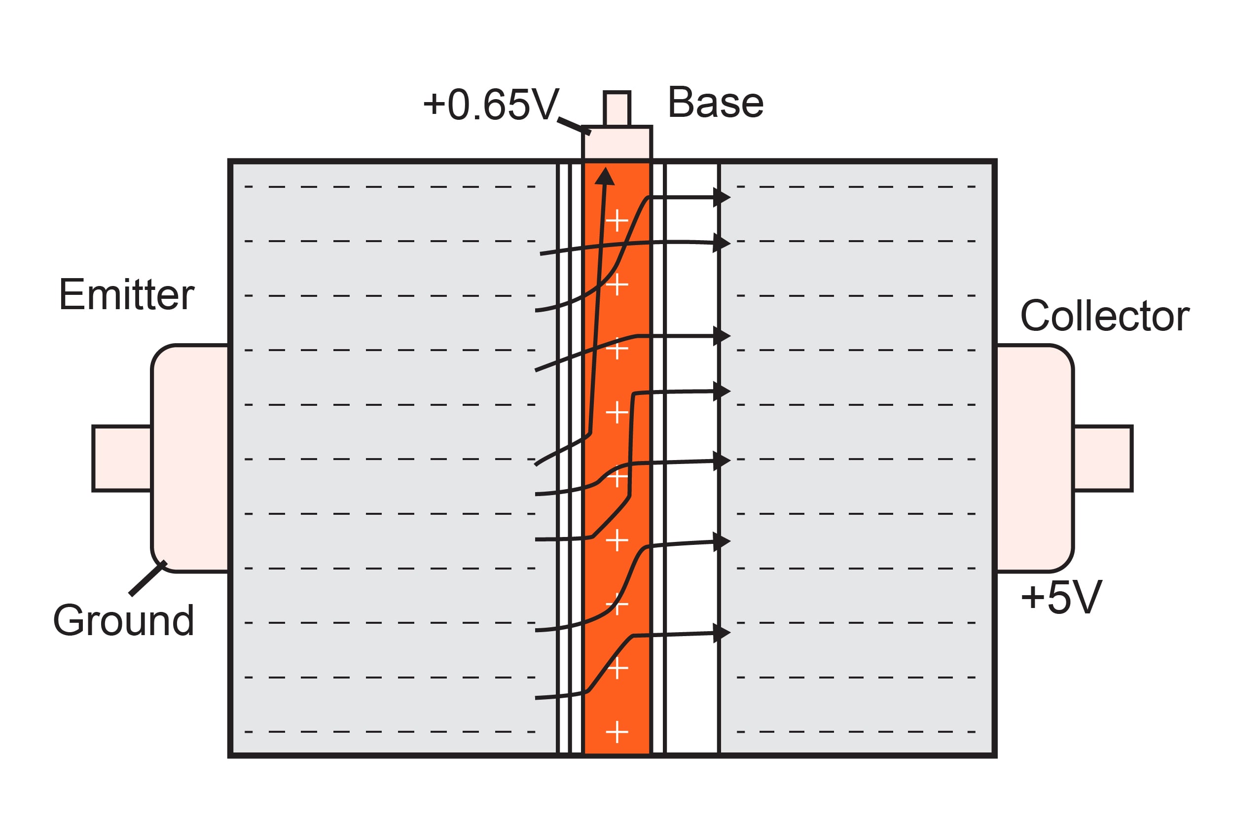
Figure 2-5. The electrons in the base of an NPN transistor are intended to flow to the base terminal. If the base is very thin, however, most of them are diverted by the positive potential of the collector.
In a good transistor, on the order of 100, or even 500, of the electrons will be sidetracked to the collector for every one that goes to the base terminal. We would thus have a current gain of 100 to 500 (Figure 2-6).
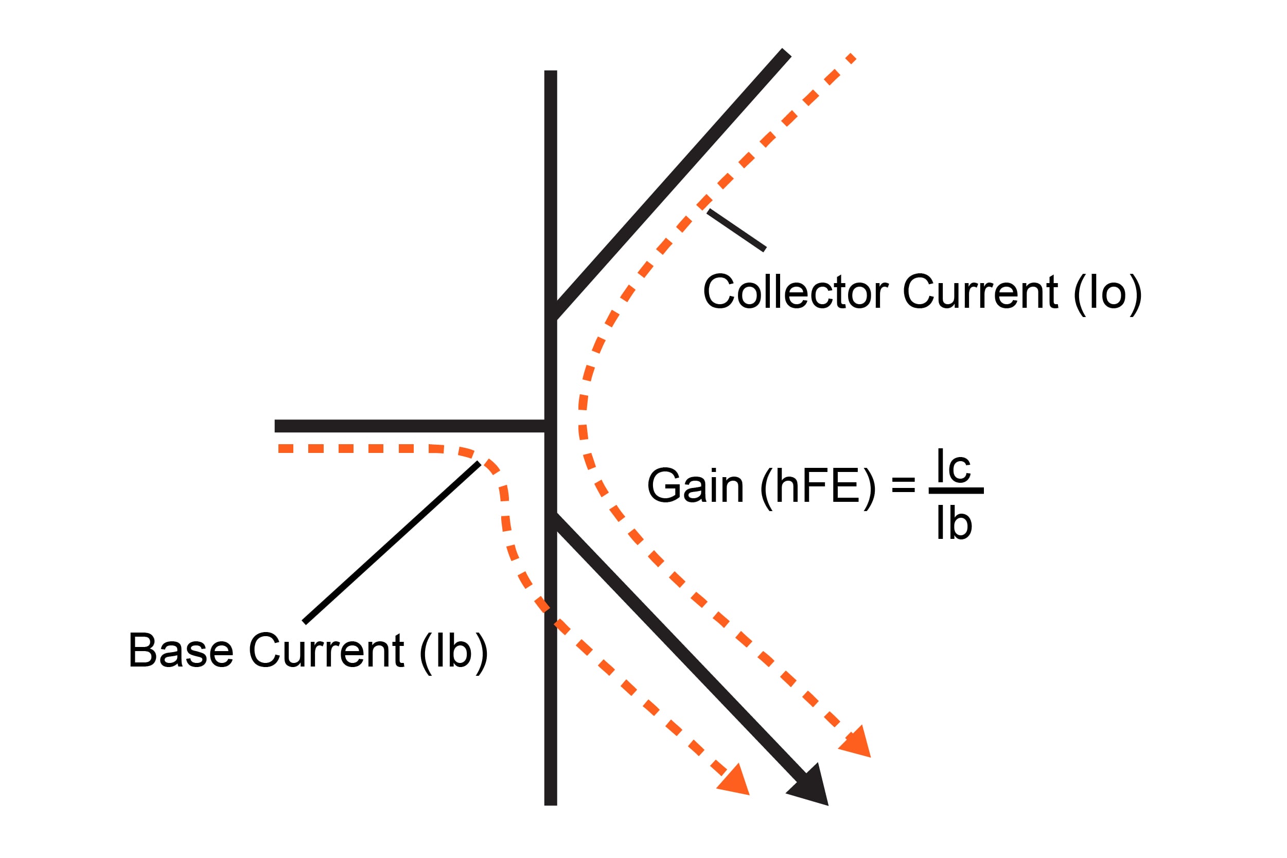
Figure 2-6. The current flow and gain of an NPN transistor.
The bipolar transistor is an odd amplifier. It’s quite nonlinear and somewhat difficult to use. Consider the input terminal, the base. With respect to the emitter, it’s a diode. You need to lift its voltage up to at least 0.6 V at room temperature for any current to flow. From that point on, the current increases exponentially in both the base and the collector.
It’s not a linear voltage amplifier—only the currents have a more or less linear relationship. Also note that because it contains both the collector and base current, the emitter current is always larger than that of the collector.
What we’ve shown here is an NPN transistor. If we reverse all the doping and the voltages, we create a PNP transistor. It works the same way in every respect except that it’s a bit handicapped: it’s slower and has a lower gain. Holes, now the minority carriers in the base, just don't move as well as electrons.
Controlled P-Type and N-Type Doping
The point-contact transistor was a nightmare to manufacture and had very poor reliability. Also, these devices were made from germanium, which has a rather limited useful temperature range. The junction transistors were made by alloying dopant materials on either side of a flat piece of germanium or silicon. It was difficult to make the base uniformly thin, and the process created considerable leakage current.
The next big step was also invented at Bell Labs: diffusion. At room temperature, gases mix even if they’re held perfectly still. This happens because each atom or molecule moves around randomly due to the thermal energy it receives. The higher the temperature, the more pronounced this movement—and thus the mixing or diffusion—is.
If the temperature is high enough (over 1,000 °C, typically), such gases can even diffuse into solid material, though their diffusion speed decreases enormously. For example, silicon exposed in a high-temperature furnace to gaseous N-type impurity atoms develops an N-layer at its surface. The N-layer’s depth is as far as the impurities penetrate. This may require a temperature close to the melting point of silicon and take several hours for a penetration of just a few micrometers (μm), but it’s far more controlled than alloying.
Moreover, you can dope repeatedly. Suppose you have a piece of silicon that has been doped N-type. If you diffuse P-type impurities into the surface, you convert the layer from N-type to P-type once there are more P-type than N-type impurities. The junction is located at the depth at which the two impurities are equal in concentration.
A second diffusion of a yet higher concentration can then convert the material back to N-type. However, you have to pay attention to the fact that subsequent exposure to high temperature causes any previous layer to diffuse further.
There are a few more dopants available, too:
- P-type gallium (rarely used).
- N-type arsenic.
- N-type antimony.
The latter two have the advantage of diffusing more slowly than phosphorus or boron. For this reason, they’re primarily used early in the process and are thus less affected by subsequent diffusions.