 Facebook
 Google
 GitHub
 Linkedin
The Cascode Amplifier
While the C-B (common-base) amplifier is known for wider bandwidth than the C-E (common-emitter) configuration, the low input impedance (10s of Ω) of C-B is a limitation for many applications. The solution is to precede the C-B stage by a low gain C-E stage which has moderately high input impedance (kΩs).
The stages are in a cascode configuration stacked in series, as opposed to cascaded for a standard amplifier chain.
“Capacitor coupled three stage common-emitter amplifier” Capacitor coupled for a cascade example. The cascode amplifier configuration has both wide bandwidth and a moderately high input impedance.
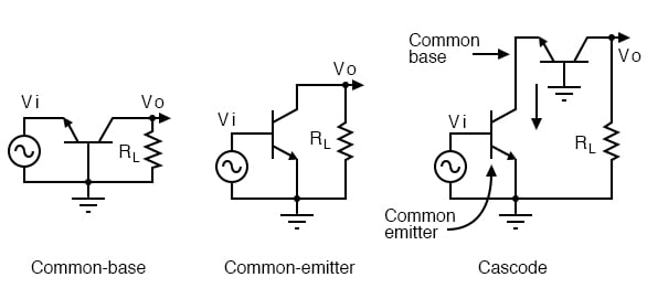
The cascode amplifier is combined common-emitter and common-base. This is an AC circuit equivalent with batteries and capacitors replaced by short circuits.
Bandwidth Capacitance and the Miller Effect
The key to understanding the wide bandwidth of the cascode configuration is the Miller effect. The Miller effect is the multiplication of the bandwidth robbing collector-base capacitance by voltage gain Av. This C-B capacitance is smaller than the E-B capacitance. Thus, one would think that the C-B capacitance would have little effect. However, in the C-E configuration, the collector output signal is out of phase with the input at the base. The collector signal capacitively coupled back opposes the base signal. Moreover, the collector feedback is (1-Av) times larger than the base signal. Keep in mind that Av is a negative number for the inverting C-E amplifier. Thus, the small C-B capacitance appears (1+|Av|) times larger than its actual value. This capacitive gain reducing feedback increases with frequency, reducing the high frequency response of a C-E amplifier.
The approximate voltage gain of the C-E amplifier in Figure below is -RL/rEE. The emitter current is set to 1.0 mA by biasing. REE= 26mV/IE = 26mV/1.0mA = 26 Ω. Thus, Av = -RL/REE = -4700/26 = -181. The pn2222 datasheet list Ccbo = 8 pF.[FAR] The miller capacitance is Ccbo(1-Av). Gain Av = -181, negative since it is inverting gain. Cmiller = Ccbo(1-Av) = 8pF(1-(-181)=1456pF
A common-base configuration is not subject to the Miller effect because the grounded base shields the collector signal from being fed back to the emitter input. Thus, a C-B amplifier has better high frequency response. To have a moderately high input impedance, the C-E stage is still desirable. The key is to reduce the gain (to about 1) of the C-E stage which reduces the Miller effect C-B feedback to 1·CCBO. The total C-B feedback is the feedback capacitance 1·CCB plus the actual capacitance CCB for a total of 2·CCBO. This is a considerable reduction from 181·CCBO. The miller capacitance for a gain of -2 C-E stage is Cmiller = Ccbo(1-Av)= Cmiller = Ccbo(1-(-1)) = Ccbo·2.
The way to reduce the common-emitter gain is to reduce the load resistance. The gain of a C-E amplifier is approximately RC/RE. The internal emitter resistance rEE at 1mA emitter current is 26Ω. For details on the 26Ω, see “Derivation of REE”, see REE. The collector load RC is the resistance of the emitter of the C-B stage loading the C-E stage, 26Ω again. CE gain amplifier gain is approximately Av = RC/RE=26/26=1. This Miller capacitance is Cmiller = Ccbo(1-Av) = 8pF(1-(-1)=16pF. We now have a moderately high input impedance C-E stage without suffering the Miller effect, but no C-E dB voltage gain. The C-B stage provides a high voltage gain, AV = -181. Current gain of cascode is β of the C-E stage, 1 for the C-B, β overall. Thus, the cascode has moderately high input impedance of the C-E, good gain, and good bandwidth of the C-B.
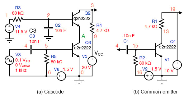
SPICE: Cascode and common-emitter for comparison.
Cascode Vs. Common-Emitter Amplifier Comparison
The SPICE version of both a cascode amplifier, and for comparison, a common-emitter amplifier is shown in Figure above. The netlist is in Table below. The AC source V3 drives both amplifiers via node 4. The bias resistors for this circuit are calculated in an example problem cascode.
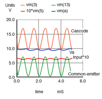
SPICE waveforms. Note that Input is multiplied by 10 for visibility.
SPICE netlist for printing AC input and output voltages.
*SPICE circuit <03502.eps> from XCircuit v3.20 V1 19 0 10 Q1 13 15 0 q2n2222 Q2 3 2 A q2n2222 R1 19 13 4.7k V2 16 0 1.5 C1 4 15 10n R2 15 16 80k Q3 A 5 0 q2n2222 V3 4 6 SIN(0 0.1 1k) ac 1 R3 1 2 80k R4 3 9 4.7k C2 2 0 10n C3 4 5 10n R5 5 6 80k V4 1 0 11.5 V5 9 0 20 V6 6 0 1.5 .model q2n2222 npn (is=19f bf=150 + vaf=100 ikf=0.18 ise=50p ne=2.5 br=7.5 + var=6.4 ikr=12m isc=8.7p nc=1.2 rb=50 + re=0.4 rc=0.3 cje=26p tf=0.5n + cjc=11p tr=7n xtb=1.5 kf=0.032f af=1) .tran 1u 5m .AC DEC 10 1k 100Meg .end
The waveforms in Figure above show the operation of the cascode stage. The input signal is displayed multiplied by 10 so that it may be shown with the outputs. Note that both the Cascode, Common-emitter, and Va (intermediate point) outputs are inverted from the input. Both the Cascode and Common emitter have large amplitude outputs. The Va point has a DC level of about 10V, about half way between 20V and ground. The signal is larger than can be accounted for by a C-E gain of 1, It is three times larger than expected.
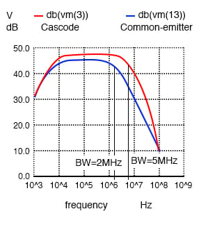
Cascode vs common-emitter banwidth.
Note: It appears that this section of the page has issues and needs to be revised. Please see the comments at the bottom of the page for more information.
Figure above shows the frequency response to both the cascode and common-emitter amplifiers. The SPICE statements responsible for the AC analysis, extracted from the listing:
V3 4 6 SIN(0 0.1 1k) ac 1 .AC DEC 10 1k 100Meg
Note the “ac 1” is necessary at the end of the V3 statement. The cascode has marginally better mid-band gain. However, we are primarily looking for the bandwidth measured at the -3dB points, down from the midband gain for each amplifier. This is shown by the vertical solid lines in Figure above. It is also possible to print the data of interest from nutmeg to the screen, the SPICE graphical viewer (command, first line):
nutmeg 6 -> print frequency db(vm(3)) db(vm(13)) Index frequency db(vm(3)) db(vm(13)) 22 0.158MHz 47.54 45.41 33 1.995MHz 46.95 42.06 37 5.012MHz 44.63 36.17
Index 22 gives the midband dB gain for Cascode vm(3)=47.5dB and Common-emitter vm(13)=45.4dB. Out of many printed lines, Index 33 was the closest to being 3dB down from 45.4dB at 42.0dB for the Common-emitter circuit. The corresponding Index 33 frequency is approximately 2Mhz, the common-emitter bandwidth. Index 37 vm(3)=44.6db is approximately 3db down from 47.5db. The corresponding Index37 frequency is 5Mhz, the cascode bandwidth. Thus, the cascode amplifier has a wider bandwidth. We are not concerned with the low frequency degradation of gain. It is due to the capacitors, which could be remedied with larger ones. The 5MHz bandwith of our cascode example, while better than the common-emitter example, is not exemplary for an RF (radio frequency) amplifier. A pair of RF or microwave transistors with lower interelectrode capacitances should be used for higher bandwidth. Before the invention of the RF dual gate MOSFET, the BJT cascode amplifier could have been found in UHF (ultra high frequency) TV tuners.
REVIEW
- A cascode amplifier consists of a common-emitter stage loaded by the emitter of a common-base stage.
- The heavily loaded C-E stage has a low gain of 1, overcoming the Miller effect
- A cascode amplifier has a high gain, moderately high input impedance, a high output impedance, and a high bandwidth.
RELATED WORKSHEETS:


Hi, I got different result. I simulate the vircuits above, the cascode one as well the common emitter one, but the result was : the blue is for the cascode, while the red is for the common emitter. I use LTSpice XVI. Pls advice.