Facebook
 Google
 GitHub
 Linkedin
Active-mode Operation (BJT)
When a transistor is in the fully-off state (like an open switch), it is said to be cutoff. Conversely, when it is fully conductive between emitter and collector (passing as much current through the collector as the collector power supply and load will allow), it is said to be saturated. These are the two modes of operation explored thus far in using the transistor as a switch.
However, bipolar transistors don’t have to be restricted to these two extreme modes of operation. As we learned in the previous section, the base current “opens a gate” for a limited amount of current through the collector. If this limit for the controlled current is greater than zero but less than the maximum allowed by the power supply and load circuit, the transistor will “throttle” the collector current in a mode somewhere between cutoff and saturation. This mode of operation is called the active mode.
Cut-off, Saturation and Active Mode
An automotive analogy for transistor operation is as follows:
Cut-off mode - is the condition of no motive force generated by the mechanical parts of the car to make it move. In cutoff mode, the brake is engaged (zero base current), preventing motion (collector current).
Active mode - is the automobile cruising at a constant, controlled speed (constant, controlled collector current) as dictated by the driver.
Saturation - the automobile driving up a steep hill that prevents it from going as fast as the driver wishes. In other words, a “saturated” automobile is one with the accelerator pedal pushed down (base current calling for more collector current than can be provided by the power supply/load circuit). Let’s set up a circuit for SPICE simulation to demonstrate what happens when a transistor is in its active mode of operation. (Figure below)
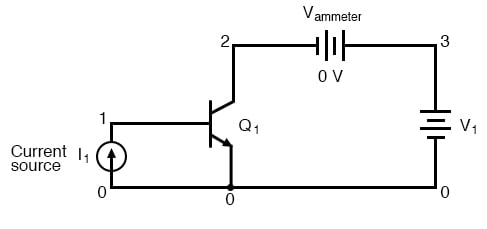
bipolar transistor simulation
i1 0 1 dc 20u
q1 2 1 0 mod1
vammeter 3 2 dc 0
v1 3 0 dc
.model mod1 npn
.dc v1 0 2 0.05
.plot dc i (vammeter)
.end
Circuit for “active mode” SPICE simulation, and netlist.
“Q” is the standard letter designation for a transistor in a schematic diagram, just as “R” is for a resistor and “C” is for a capacitor. In this circuit, we have an NPN transistor powered by a battery (V1) and controlled by the current through a current source (I1).
A current source is a device that outputs a specific amount of current, generating as much or as little voltage across its terminals to ensure that the exact amount of current through it. Current sources are notoriously difficult to find in nature (unlike voltage sources, which by contrast attempt to maintain a constant voltage, outputting as much or as little current in the fulfillment of that task), but can be simulated with a small collection of electronic components. As we are about to see, transistors themselves tend to mimic the constant-current behavior of a current source in their ability to regulate current at a fixed value.
In the SPICE simulation, we’ll set the current source (I1) at a constant value of 20 µA, then vary the voltage source (V1) over a range of 0 to 2 volts and monitor how much current goes through it. The “dummy” battery (Vammeter) in the figure above with its output of 0 volts serves merely to provide SPICE with a circuit element for current measurement.
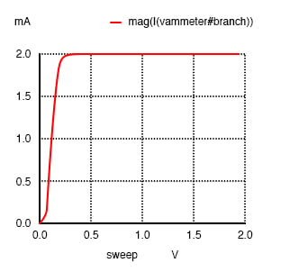
A Sweeping collector voltage 0 to 2 V with base current constant at 20 µA yields constant 2 mA collector current in the saturation region.
The constant base current of 20 µA sets a collector current limit of 2 mA, exactly 100 times as much. Notice how flat the curve is in (Figure above) for collector current over the range of battery voltage from 0 to 2 volts. The only exception to this featureless plot is at the very beginning, where the battery increases from 0 volts to 0.25 volts. There, the collector current increases rapidly from 0 amps to its limit of 2 mA.
Let’s see what happens if we vary the battery voltage over a wider range, this time from 0 to 50 volts. We’ll keep the base current steady at 20 µA. (Figure below)
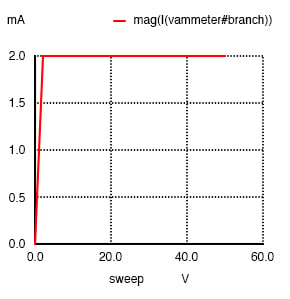
bipolar transistor simulation
i1 0 1 dc 20u
q1 2 1 0 mod1
vammeter 3 2 dc 0
v1 3 0 dc
.model mod1 npn
.dc v1 0 50 2
.plot dc i (vammeter)
.end
Sweeping collector voltage 0 to 50 V with base current constant at 20 µA yields constant 2 mA collector current.
Same result! The collector current in the figure above holds steady at 2 mA, although the battery (v1) voltage varies from 0 to 50 volts. It would appear from our simulation that collector-to-emitter voltage has little effect over collector current, except at very low levels (just above 0 volts). The transistor is acting as a current regulator, allowing exactly 2 mA through the collector and no more.
Now let’s see what happens if we increase the controlling (I1) current from 20 µA to 75 µA, once again sweeping the battery (V1) voltage from 0 to 50 volts and graphing the collector current in Figure below.
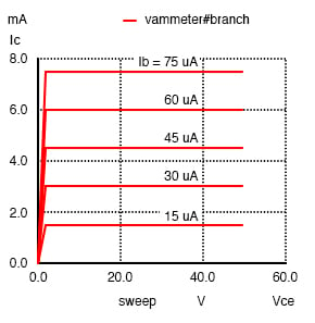
bipolar transistor simulation
i1 0 1 dc 75u
q1 2 1 0 mod1
vammeter 3 2 dc 0
v1 3 0 dc
.model mod1 npn
.dc v1 0 50 2 i1 15u 75u 15u
.plot dc i (vammeter)
.end
Sweeping collector voltage 0 to 50 V (.dc v1 0 50 2) with base current constant at 75 µA yields constant 7.5 mA collector current. Other curves are generated by current sweep (i1 15u 75u 15u) in DC analysis statement (.dc v1 0 50 2 i1 15u 75u 15u).
Not surprisingly, SPICE gives us a similar plot: a flat line, holding steady this time at 7.5 mA—exactly 100 times the base current—over the range of battery voltages from just above 0 volts to 50 volts. It appears that the base current is the deciding factor for collector current, the V1 battery voltage being irrelevant as long as it is above a certain minimum level.
This voltage/current relationship is entirely different from what we’re used to seeing across a resistor. With a resistor, current increases linearly as the voltage across it increases. Here, with a transistor, current from emitter to collector stays limited at a fixed, maximum value no matter how high the voltage across the emitter and collector increases.
Often it is useful to superimpose several collector current/voltage graphs for different base currents on the same graph as in the figure below. A collection of curves like this—one curve plotted for each distinct level of base current—for a particular transistor is called the transistor’s characteristic curves:
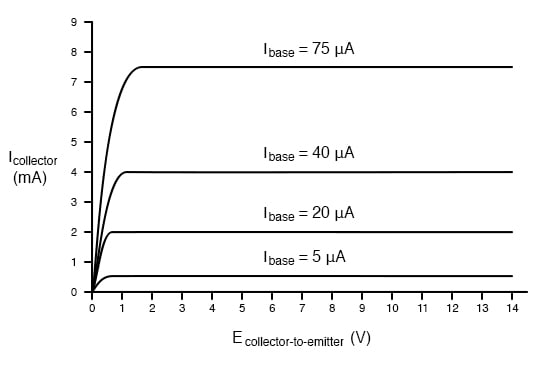
Collector current versus collector-emitter voltage for various base currents.
Each curve on the graph reflects the collector current of the transistor, plotted over a range of collector-to-emitter voltages, for a given amount of base current. Since a transistor tends to act as a current regulator, limiting collector current to a proportion set by the base current, it is useful to express this proportion as a standard transistor performance measure. Specifically, the ratio of collector current to base current is known as the Beta ratio (symbolized by the Greek letter β):
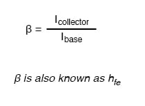
Sometimes the β ratio is designated as “hfe,” a label used in a branch of mathematical semiconductor analysis known as “hybrid parameters” which strives to achieve precise predictions of transistor performance with detailed equations. Hybrid parameter variables are many, but each is labeled with the general letter “h” and a specific subscript. The variable “hfe” is just another (standardized) way of expressing the ratio of collector current to base current, and is interchangeable with “β.” The β ratio is unitless.
β for any transistor is determined by its design: it cannot be altered after manufacture. It is rare to have two transistors of the same design exactly match because of the physical variables affecting β. If a circuit design relies on equal β ratios between multiple transistors, “matched sets” of transistors may be purchased at extra cost. However, it is generally considered bad design practice to engineer circuits with such dependencies.
The β of a transistor does not remain stable for all operating conditions. For an actual transistor, the β ratio may vary by a factor of over 3 within its operating current limits. For example, a transistor with advertised β of 50 may test with Ic/Ib ratios as low as 30 and as high as 100, depending on the amount of collector current, the transistor’s temperature, and frequency of the amplified signal, among other factors. For tutorial purposes it is adequate to assume a constant β for any given transistor; realize that real life is not that simple!
Sometimes it is helpful for comprehension to “model” complex electronic components with a collection of simpler, better-understood components. The model in the figure below is used in many introductory electronics texts.
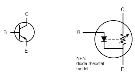
Elementary diode-resistor transistor model.
This model casts the transistor as a combination of diode and rheostat (variable resistor). Current through the base-emitter diode controls the resistance of the collector-emitter rheostat (as implied by the dashed line connecting the two components), thus controlling collector current. An NPN transistor is modeled in the figure shown, but a PNP transistor would be only slightly different (only the base-emitter diode would be reversed).
This model succeeds in illustrating the basic concept of transistor amplification: how the base current signal can exert control over the collector current. However, the model miscommunicates the notion of a set amount of collector-emitter resistance for a given amount of base current. If this were true, the transistor wouldn’t regulate collector current at all as the characteristic curves show. Instead of the collector current curves flattening out after their brief rise as the collector-emitter voltage increases, the collector current would be directly proportional to collector-emitter voltage, rising steadily in a straight line on the graph.
A better transistor model, often seen in more advanced textbooks, is shown in figure below.
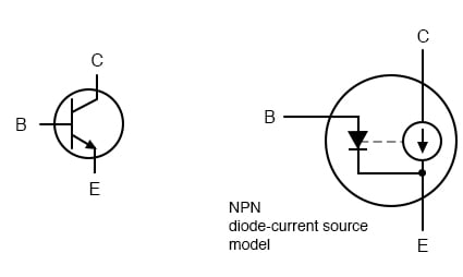
Current source model of transistor.
It casts the transistor as a combination of a diode and current source, the output of the current source being set at a multiple (β ratio) of the base current. This model is far more accurate in depicting the true input/output characteristics of a transistor: base current establishes a certain amount of collector current, rather than a certain amount of collector-emitter resistance as the first model implies. Also, this model is favored when performing network analysis on transistor circuits, the current source being a well-understood theoretical component. Unfortunately, using a current source to model the transistor’s current-controlling behavior can be misleading: in no way will the transistor ever act as a source of electrical energy. The current source does not model the fact that its source of energy is an external power supply, similar to an amplifier.
REVIEW:
- A transistor is said to be in its active mode if it is operating somewhere between fully on (saturated) and fully off (cutoff).
- Base current regulates collector current. By regulate, we mean that no more collector current can exist than what is allowed by the base current.
- The ratio between collector current and base current is called “Beta” (β) or “hfe”.
- β ratios are different for every transistor, and
- β changes for different operating conditions.
RELATED WORKSHEETS: