 Facebook
 Google
 GitHub
 Linkedin
Shift Registers: Parallel-in, Serial-out (PISO) Conversion
Parallel-in/ serial-out shift registers do everything that the previous serial-in/ serial-out shift registers do plus input data to all stages simultaneously.
The parallel-in/ serial-out shift register stores data, shifts it on a clock by clock basis, and delays it by the number of stages times the clock period.
In addition, parallel-in/ serial-out really means that we can load data in parallel into all stages before any shifting ever begins.
This is a way to convert data from a parallel format to a serial format. By parallel format we mean that the data bits are present simultaneously on individual wires, one for each data bit as shown below.
By serial format we mean that the data bits are presented sequentially in time on a single wire or circuit as in the case of the “data out” on the block diagram below.

Below we take a close look at the internal details of a 3-stage parallel-in/ serial-out shift register.
A stage consists of a type D Flip-Flop for storage, and an AND-OR selector to determine whether data will load in parallel, or shift stored data to the right.
In general, these elements will be replicated for the number of stages required. We show three stages due to space limitations.
Four, eight or sixteen bits is normal for real parts.
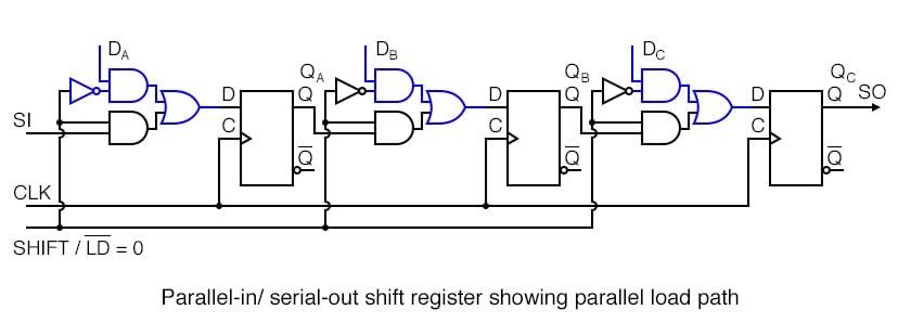
Above we show the parallel load path when SHIFT/LD’ is logic low. The upper NAND gates serving DA DB DC are enabled, passing data to the D inputs of type D Flip-Flops QA QB DC respectively.
At the next positive going clock edge, the data will be clocked from D to Q of the three FFs. Three bits of data will load into QA QB DC at the same time.
The type of parallel load just described, where the data loads on a clock pulse is known as synchronous load because the loading of data is synchronized to the clock.
This needs to be differentiated from asynchronous load where loading is controlled by the preset and clear pins of the Flip-Flops which does not require the clock.
Only one of these load methods is used within an individual device, the synchronous load being more common in newer devices.
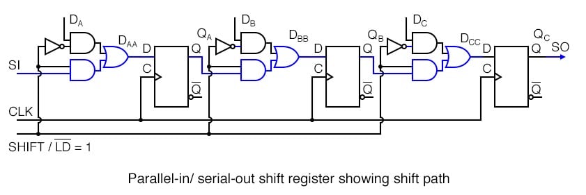
The shift path is shown above when SHIFT/LD’ is logic high. The lower AND gates of the pairs feeding the OR gate are enabled giving us a shift register connection of SI to DA , QA to DB , QB to DC , QC to SO. Clock pulses will cause data to be right shifted out to SO on successive pulses.
The waveforms below show both parallel loading of three bits of data and serial shifting of this data. Parallel data at DA DB DC is converted to serial data at SO.

What we previously described with words for parallel loading and shifting is now set down as waveforms above.
As an example we present 101 to the parallel inputs DAA DBB DCC. Next, the SHIFT/LD’ goes low enabling loading of data as opposed to shifting of data.
It needs to be low a short time before and after the clock pulse due to setup and hold requirements. It is considerably wider than it has to be.
Though, with synchronous logic it is convenient to make it wide. We could have made the active low SHIFT/LD’ almost two clocks wide, low almost a clock before t1 and back high just before t3.
The important factor is that it needs to be low around clock time t1 to enable parallel loading of the data by the clock.
Note that at t1 the data 101 at DA DB DC is clocked from D to Q of the Flip-Flops as shown at QA QB QC at time t1.
This is the parallel loading of the data synchronous with the clock.

Now that the data is loaded, we may shift it provided that SHIFT/LD’ is high to enable shifting, which it is prior to t2.
At t2 the data 0 at QC is shifted out of SO which is the same as the QC waveform. It is either shifted into another integrated circuit, or lost if there is nothing connected to SO.
The data at QB, a 0 is shifted to QC. The 1 at QA is shifted into QB. With “data in” a 0, QA becomes 0. After t2, QA QB QC = 010.
After t3, QA QB QC = 001. This 1, which was originally present at QA after t1, is now present at SO and QC.
The last data bit is shifted out to an external integrated circuit if it exists. After t4 all data from the parallel load is gone.
At clock t5 we show the shifting in of a data 1 present on the SI, serial input.
Q: Why provide SI and SO pins on a shift register?
A: These connections allow us to cascade shift register stages to provide large shifters than available in a single IC (Integrated Circuit) package. They also allow serial connections to and from other ICs like microprocessors.
Let’s take a closer look at parallel-in/ serial-out shift registers available as integrated circuits, courtesy of Texas Instruments.
For complete device data sheets follow these the links.
Parallel-in/serial-out devices
- SN74ALS166 parallel-in/ serial-out 8-bit shift register, synchronous load
- SN74ALS165 parallel-in/ serial-out 8-bit shift register, asynchronous load
- CD4014B parallel-in/ serial-out 8-bit shift register, synchronous load
- SN74LS647 parallel-in/ serial-out 16-bit shift register, synchronous load

The SN74ALS166 shown above is the closest match of an actual part to the previous parallel-in/ serial out shifter figures.
Let us note the minor changes to our figure above. First of all, there are 8-stages. We only show three.
All 8-stages are shown on the data sheet available at the link above. The manufacturer labels the data inputs A, B, C, and so on to H.
The SHIFT/LOAD control is called SH/LD’. It is abbreviated from our previous terminology, but works the same: parallel load if low, shift if high.
The shift input (serial data in) is SER on the ALS166 instead of SI. The clock CLK is controlled by an inhibit signal, CLKINH.
If CLKINH is high, the clock is inhibited, or disabled. Otherwise, this “real part” is the same as what we have looked at in detail.

Above is the ANSI (American National Standards Institute) symbol for the SN74ALS166 as provided on the data sheet.
Once we know how the part operates, it is convenient to hide the details within a symbol. There are many general forms of symbols.
The advantage of the ANSI symbol is that the labels provide hints about how the part operates.
The large notched block at the top of the ‘74ASL166 is the control section of the ANSI symbol. There is a reset indicted by R.
There are three control signals: M1 (Shift), M2 (Load), and C3/1 (arrow) (inhibited clock). The clock has two functions.
First, C3 for shifting parallel data wherever a prefix of 3 appears. Second, whenever M1 is asserted, as indicated by the 1 of C3/1 (arrow), the data is shifted as indicated by the right pointing arrow.
The slash (/) is a separator between these two functions. The 8-shift stages, as indicated by title SRG8, are identified by the external inputs A, B, C, to H.
The internal 2, 3D indicates that data, D, is controlled by M2 [Load] and C3 clock. In this case, we can conclude that the parallel data is loaded synchronously with the clock C3.
The upper stage at A is a wider block than the others to accommodate the input SER.
The legend 1, 3D implies that SER is controlled by M1 [Shift] and C3 clock. Thus, we expect to clock in data at SER when shifting as opposed to parallel loading.

The ANSI/IEEE basic gate rectangular symbols are provided above for comparison to the more familiar shape symbols so that we may decipher the meaning of the symbology associated with the CLKINH and CLKpins on the previous ANSI SN74ALS166 symbol.
The CLK and CLKINH feed an OR gate on the SN74ALS166 ANSI symbol. OR is indicated by => on the rectangular inset symbol.
The long triangle at the output indicates a clock. If there was a bubble with the arrow this would have indicated shift on negative clock edge (high to low).
Since there is no bubble with the clock arrow, the register shifts on the positive (low to high transition) clock edge.
The long arrow, after the legend C3/1 pointing right indicates shift right, which is down the symbol.

Part of the internal logic of the SN74ALS165 parallel-in/ serial-out, asynchronous load shift register is reproduced from the data sheet above.
See the link at the beginning of this section the for the full diagram. We have not looked at asynchronous loading of data up to this point.
First of all, the loading is accomplished by application of appropriate signals to the Set (preset) and Reset (clear) inputs of the Flip-Flops.
The upper NAND gates feed the Set pins of the FFs and also cascades into the lower NAND gate feeding the Reset pins of the FFs.
The lower NAND gate inverts the signal in going from the Set pin to the Reset pin.
First, SH/LD’ must be pulled Low to enable the upper and lower NAND gates.
If SH/LD’ were at a logic high instead, the inverter feeding a logic low to all NAND gates would force a High out, releasing the “active low” Set and Reset pins of all FFs.
There would be no possibility of loading the FFs.
With SH/LD’ held Low, we can feed, for example, a data 1 to parallel input A, which inverts to a zero at the upper NAND gate output, setting FF QA to a 1.
The 0 at the Set pin is fed to the lower NAND gate where it is inverted to a 1 , releasing the Reset pin of QA.
Thus, a data A=1 sets QA=1. Since none of this required the clock, the loading is asynchronous with respect to the clock.
We use an asynchronous loading shift register if we cannot wait for a clock to parallel load data, or if it is inconvenient to generate a single clock pulse.
The only difference in feeding a data 0 to parallel input A is that it inverts to a 1 out of the upper gate releasing Set.
This 1 at Set is inverted to a 0 at the lower gate, pulling Reset to a Low, which resets QA=0.

The ANSI symbol for the SN74ALS166 above has two internal controls C1 [LOAD] and C2 clock from the OR function of (CLKINH, CLK).
SRG8 says 8-stage shifter. The arrow after C2 indicates shifting right or down. SER input is a function of the clock as indicated by internal label 2D.
The parallel data inputs A, B, C to H are a function of C1 [LOAD], indicated by internal label 1D.
C1 is asserted when sh/LD’ =0 due to the half-arrow inverter at the input.
Compare this to the control of the parallel data inputs by the clock of the previous synchronous ANSI SN75ALS166. Note the differences in the ANSI Data labels.

On the CD4014B above, M1 is asserted when LD/SH’=0. M2 is asserted when LD/SH’=1.
Clock C3/1 is used for parallel loading data at 2, 3D when M2 is active as indicated by the 2,3 prefix labels.
Pins P3 to P7 are understood to have the smae internal 2,3 prefix labels as P2 and P8. At SER, the 1,3D prefix implies that M1 and clock C3 are necessary to input serial data.
Right shifting takes place when M1 active is as indicated by the 1 in C3/1 arrow.
The CD4021B is a similar part except for asynchronous parallel loading of data as implied by the lack of any 2 prefix in the data label 1D for pins P1, P2, to P8.
Of course, prefix 2 in label 2D at input SER says that data is clocked into this pin. The OR gate inset shows that the clock is controlled by LD/SH’.

The above SN74LS674 internal label SRG 16 indicates 16-bit shift register.
The MODE input to the control section at the top of the symbol is labeled 1,2 M3. Internal M3 is a function of input MODE and G1 and G2as indicated by the 1,2 preceding M3.
The base label G indicates an AND function of any such G inputs. Input R/W’ is internally labeled G1/2 EN.
This is an enable EN (controlled by G1 AND G2) for tristate devices used elsewhere in the symbol.
We note that CS’ on (pin 1) is internal G2. Chip select CS’ also is ANDed with the input CLK to give internal clock C4.
The bubble within the clock arrow indicates that activity is on the negative (high to low transition) clock edge.
The slash (/) is a separator implying two functions for the clock. Before the slash, C4 indicates control of anything with a prefix of 4.
After the slash, the 3’ (arrow) indicates shifting. The 3’ of C4/3’ implies shifting when M3 is de-asserted (MODE=0). The long arrow indicates shift right (down).
Moving down below the control section to the data section, we have external inputs P0-P15, pins (7-11, 13-23).
The prefix 3,4 of internal label 3,4D indicates that M3 and the clock C4 control loading of parallel data.
The D stands for Data. This label is assumed to apply to all the parallel inputs, though not explicitly written out.
Locate the label 3’,4D on the right of the P0 (pin7) stage. The complemented-3 indicates thatM3=MODE=0 inputs (shifts) SER/Q15 (pin5) at clock time, (4 of 3’,4D) corresponding to clock C4.
In other words, with MODE=0, we shift data into Q0 from the serial input (pin 6). All other stages shift right (down) at clock time.
Moving to the bottom of the symbol, the triangle pointing right indicates a buffer between Q and the output pin.
The Triangle pointing down indicates a tri-state device. We previously stated that the tristate is controlled by enable EN, which is actually G1 AND G2 from the control section.
If R/W=0, the tri-state is disabled, and we can shift data into Q0 via SER (pin 6), a detail we omitted above. We actually need MODE=0, R/W’=0, CS’=0
The internal logic of the SN74LS674 and a table summarizing the operation of the control signals is available in the link in the bullet list, top of section.
If R/W’=1, the tristate is enabled, Q15 shifts out SER/Q15 (pin 6) and recirculates to the Q0 stage via the right hand wire to 3’,4D.
We have assumed that CS’ was low giving us clock C4/3’ and G2 to ENable the tri-state.
Practical Applications
An application of a parallel-in/ serial-out shift register is to read data into a microprocessor.

The Alarm above is controlled by a remote keypad. The alarm box supplies +5V and ground to the remote keypad to power it.
The alarm reads the remote keypad every few tens of milliseconds by sending shift clocks to the keypad which returns serial data showing the status of the keys via a parallel-in/ serial-out shift register.
Thus, we read nine key switches with four wires. How many wires would be required if we had to run a circuit for each of the nine keys?

A practical application of a parallel-in/ serial-out shift register is to read many switch closures into a microprocessor on just a few pins.
Some low end microprocessors only have 6-I/O (Input/Output) pins available on an 8-pin package.
Or, we may have used most of the pins on an 84-pin package. We may want to reduce the number of wires running around a circuit board, machine, vehicle, or building.
This will increase the reliability of our system. It has been reported that manufacturers who have reduced the number of wires in an automobile produce a more reliable product.
In any event, only three microprocessor pins are required to read in 8-bits of data from the switches in the figure above.
We have chosen an asynchronous loading device, the CD4021B because it is easier to control the loading of data without having to generate a single parallel load clock.
The parallel data inputs of the shift register are pulled up to +5V with a resistor on each input.
If all switches are open, all 1s will be loaded into the shift register when the microprocessor moves the LD/SH’ line from low to high, then back low in anticipation of shifting.
Any switch closures will apply logic 0s to the corresponding parallel inputs. The data pattern at P1-P7 will be parallel loaded by the LD/SH’=1 generated by the microprocessor software.
The microprocessor generates shift pulses and reads a data bit for each of the 8-bits.
This process may be performed totally with software, or larger microprocessors may have one or more serial interfaces to do the task more quickly with hardware.
With LD/SH’=0, the microprocessor generates a 0 to 1 transition on the Shift clock line, then reads a data bit on the Serial data in line. This is repeated for all 8-bits.
The SER line of the shift register may be driven by another identical CD4021B circuit if more switch contacts need to be read.
In which case, the microprocessor generates 16-shift pulses. More likely, it will be driven by something else compatible with this serial data format, for example, an analog to digital converter, a temperature sensor, a keyboard scanner, a serial read-only memory.
As for the switch closures, they may be limit switches on the carriage of a machine, an over-temperature sensor, a magnetic reed switch, a door or window switch, an air or water pressure switch, or a solid state optical interrupter.
RELATED WORKSHEETS:


