Facebook
 Google
 GitHub
 Linkedin
TTL NAND and AND gates
Suppose we altered our basic open-collector inverter circuit, adding a second input terminal just like the first:
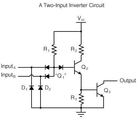
This schematic illustrates a real circuit, but it isn’t called a “two-input inverter.” Through analysis, we will discover what this Circuit’s logic function is and correspondingly what it should be designated as.
Just as in the case of the inverter and buffer, the “steering” diode cluster marked “Q1” is actually formed like a transistor, even though it isn’t used in any amplifying capacity. Unfortunately, a simple NPN transistor structure is inadequate to simulate the three PN junctions necessary in this diode network, so a different transistor (and symbol) is needed.
This transistor has one collector, one base, and two emitters, and in the circuit, it looks like this:
In the single-input (inverter) circuit, grounding the input resulted in an output that assumed the “high” (1) state. In the case of the open-collector output configuration, this “high” state was simply “floating.”
Allowing the input to float (or be connected to Vcc) resulted in the output becoming grounded, which is the “low” or 0 state. Thus, a 1 in resulted in a 0 out, and vice versa.
Circuit Illustration for Input States
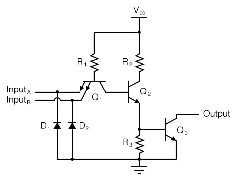
Since this circuit bears so much resemblance to the simple inverter circuit, the only difference being a second input terminal connected in the same way to the base of transistor Q2, we can say that each of the inputs will have the same effect on the output.
Namely, if either of the inputs is grounded, transistor Q2 will be forced into a condition of cutoff, thus turning Q3 off and floating the output (output goes “high”). The following series of illustrations shows this for three input states (00, 01, and 10):
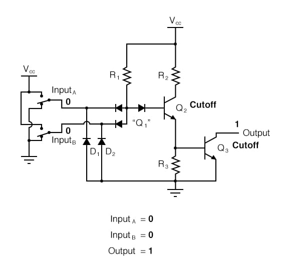
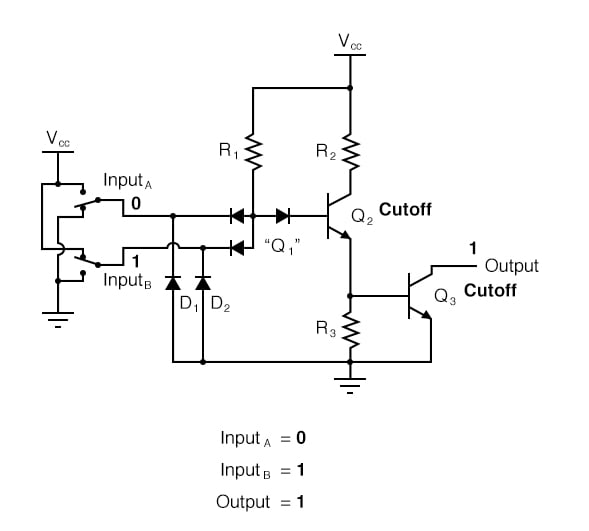
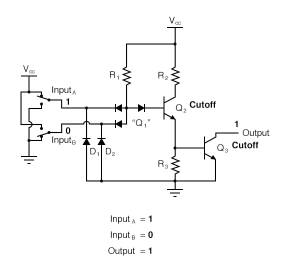
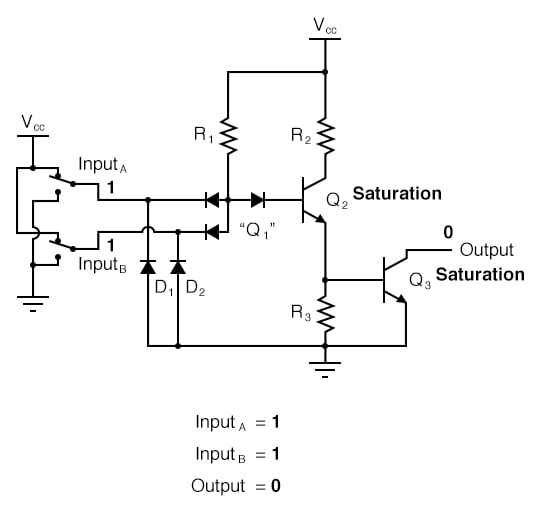
In any case, where there is a grounded (“low”) input, the output is guaranteed to be floating (“high”). Conversely, the only time the output will ever go “low” is if transistor Q3 turns on, which means transistor Q2 must be turned on (saturated), which means neither input can be diverting R1current away from the base of Q2.
The only condition that will satisfy this requirement is when both inputs are “high” (1):
NAND Gate
Collecting and tabulating these results into a truth table, we see that the pattern matches that of the NAND gate:
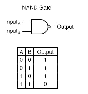
In the earlier section on NAND gates, this type of gate was created by taking an AND gate and increasing its complexity by adding an inverter (NOT gate) to the output. However, when we examine this circuit, we see that the NAND function is actually the simplest, most natural mode of operation for this TTL design.
To create an AND function using TTL circuitry, we need to increase the complexity of this circuit by adding an inverter stage to the output, just like we had to add an additional transistor stage to the TTL inverter circuit to turn it into a buffer:
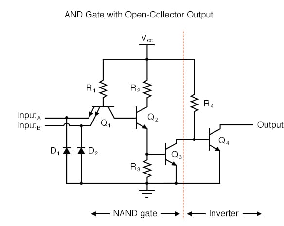
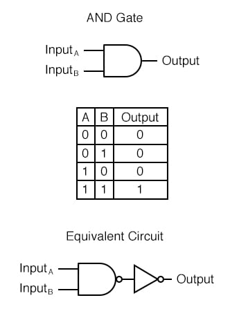
AND Gate
The truth table and equivalent gate circuit (an inverted-output NAND gate) are shown here:
Of course, both NAND and AND gate circuits may be designed with totem-pole output stages rather than open-collector. I am opting to show the open-collector versions for the sake of simplicity.
REVIEW:
- A TTL NAND gate can be made by taking a TTL inverter circuit and adding another input.
- An AND gate may be created by adding an inverter stage to the output of the NAND gate circuit.
RELATED WORKSHEET: