 Facebook
 Google
 GitHub
 Linkedin
The “Buffer” Gate
If we were to connect two inverter gates together so that the output of one fed into the input of another, the two inversion functions would “cancel” each other out so that there would be no inversion from input to final output:
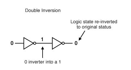
While this may seem like a pointless thing to do, it does have practical application. Remember that gate circuits are signal amplifiers, regardless of what logic function they may perform.
A weak signal source (one that is not capable of sourcing or sinking very much current to a load) may be boosted by means of two inverters like the pair shown in the previous illustration. The logic level is unchanged, but the full current-sourcing or sinking capabilities of the final inverter are available to drive a load resistance if needed.
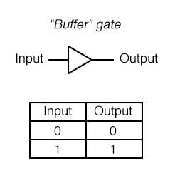
For this purpose, a special logic gate called a buffer is manufactured to perform the same function as two inverters. Its symbol is simply a triangle, with no inverting “bubble” on the output terminal:
Buffer Circuit with Open-Collector Output
The internal schematic diagram for a typical open-collector buffer is not much different from that of a simple inverter: only one more common-emitter transistor stage is added to re-invert the output signal.
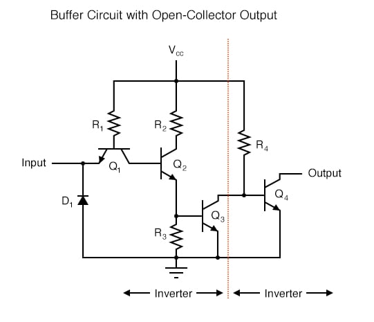
“High” Input Analysis
Let’s analyze this circuit for two conditions: an input logic level of “1” and an input logic level of “0.” First, a “high” (1) input:
As before with the inverter circuit, the “high” input causes no conduction through the left steering diode of Q1 (emitter-to-base PN junction). All of R1‘s current goes through the base of transistor Q2, saturating it:
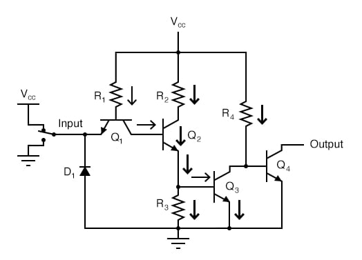
Having Q2 saturated causes Q3 to be saturated as well, resulting in very little voltage dropped between the base and emitter of the final output transistor Q4. Thus, Q4 will be in cutoff mode, conducting no current.
The output terminal will be floating (neither connected to ground nor Vcc), and this will be equivalent to a “high” state on the input of the next TTL gate that this one feeds in to. Thus, a “high” input gives a “high” output.
“Low” Input Analysis
With a “low” input signal (input terminal grounded), the analysis looks something like this:
All of R1‘s current is now diverted through the input switch, thus eliminating base current through Q2. This forces transistor Q2 into cutoff so that no base current goes through Q3 either.
With Q3 cutoff as well, Q4 is will be saturated by the current through resistor R4, thus connecting the output terminal to ground, making it a “low” logic level. Thus, a “low” input gives a “low” output.
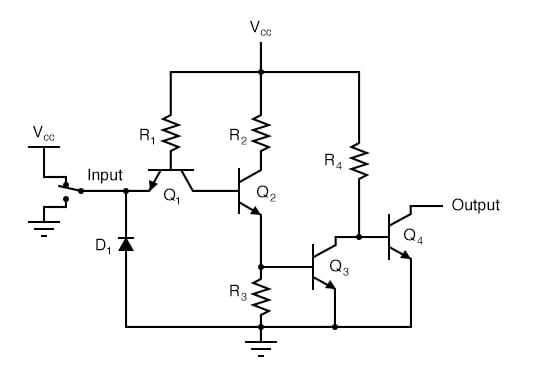
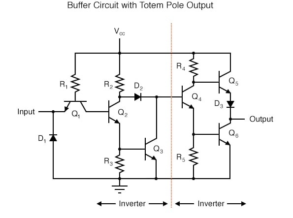
Schematic Diagram with Totem Pole Output Transistors
The schematic diagram for a buffer circuit with totem pole output transistors is a bit more complex, but the basic principles, and certainly the truth table, are the same as for the open-collector circuit:
REVIEW:
- Two inverter, or NOT, gates connected in “series” so as to invert, then re-invert, a binary bit perform the function of a buffer. Buffer gates merely serve the purpose of signal amplification: taking a “weak” signal source that isn’t capable of sourcing or sinking much current, and boosting the current capacity of the signal so as to be able to drive a load.
- Buffer circuits are symbolized by a triangle symbol with no inverter “bubble.”
- Buffers, like inverters, may be made in open-collector output or totem pole output forms.
RELATED WORKSHEET:


Thank man/ladie!
Still have a question: why we need R3? emitor of Q2 why can’t drive direct base of Q3! we have R2 for rest of voltage of Vcc!
So what accounts for the voltage drop from inputs to output