 Facebook
 Google
 GitHub
 Linkedin
TTL NOR and OR gates
TTL Circuit Analysis
Let’s examine the following TTL circuit and analyze its operation:
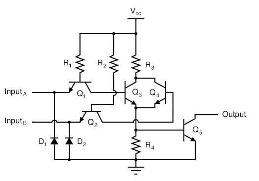
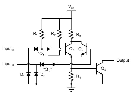
Transistors Q1 and Q2 are both arranged in the same manner that we’ve seen for transistor Q1 in all the other TTL circuits. Rather than functioning as amplifiers, Q1 and Q2 are both being used as two-diode “steering” networks. We may replace Q1 and Q2 with diode sets to help illustrate:
If input A is left floating (or connected to Vcc), current will go through the base of transistor Q3, saturating it. If input A is grounded, that current is diverted away from Q3‘s base through the left steering diode of “Q1,” thus forcing Q3 into cutoff. The same can be said for input B and transistor Q4: the logic level of input B determines Q4‘s conduction: either saturated or cutoff.
Notice how transistors Q3 and Q4 are paralleled at their collector and emitter terminals. In essence, these two transistors are acting as paralleled switches, allowing current through resistors R3 and R4 according to the logic levels of inputs A and B. If any input is at a “high” (1) level, then at least one of the two transistors (Q3 and/or Q4) will be saturated, allowing current through resistors R3 and R4, and turning on the final output transistor Q5 for a “low” (0) logic level output. The only way the output of this circuit can ever assume a “high” (1) state is if both Q3 and Q4 are cut off, which means both inputs would have to be grounded, or “low” (0).
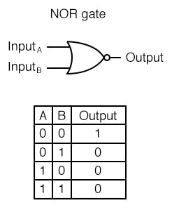
NOR Gate Truth Table
This circuit’s truth table, then, is equivalent to that of the NOR gate:
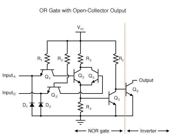
Converting a NOR Gate TTL Circuit into an OR Gate
In order to turn this NOR gate circuit into an OR gate, we would have to invert the output logic level with another transistor stage, just like we did with the NAND-to-AND gate example:
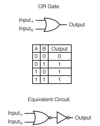
OR Gate Truth Table
The truth table and equivalent gate circuit (an inverted-output NOR gate) are shown here:
Of course, totem-pole output stages are also possible in both NOR and OR TTL logic circuits.
REVIEW:
- An OR gate may be created by adding an inverter stage to the output of the NOR gate circuit.


How do I know resistors values? I need to implement TTL OR gate circuit on a breadboard