Facebook
 Google
 GitHub
 Linkedin
Diode Switching Circuits
Diodes can perform switching and digital logic operations. Forward and reverse bias switch a diode between the low and high impedance states, respectively. Thus, it serves as a switch.
Logic
Diodes can perform digital logic functions: AND, and OR. Diode logic was used in early digital computers. It only finds limited application today. Sometimes it is convenient to fashion a single logic gate from a few diodes.
AND Gate
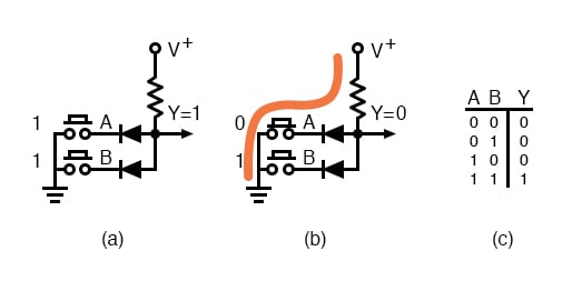
Diode AND gate
An AND gate is shown in the figure above. Logic gates have inputs and an output (Y) which is a function of the inputs. The inputs to the gate are high (logic 1), say 10 V, or low, 0 V (logic 0).
In the figure, the logic levels are generated by switches. If a switch is up, the input is effectively high (1). If the switch is down, it connects a diode cathode to ground, which is low (0). The output depends on the combination of inputs at A and B. The inputs and output are customarily recorded in a “truth table” at (c) to describe the logic of a gate. At (a) all inputs are high (1). This is recorded in the last line of the truth table at (c).
The output, Y, is high (1) due to the V+ on the top of the resistor. It is unaffected by open switches. At (b) switch A pulls the cathode of the connected diode low, pulling output Y low (0.7 V). This is recorded in the third line of the truth table.
The second line of the truth table describes the output with the switches reversed from (b). Switch B pulls the diode and output low. The first line of the truth table records the Output=0 for both input low (0).
The truth table describes a logical AND function. Summary: both inputs A and B high yields a high (1) out.
OR gate
A two input OR gate composed of a pair of diodes is shown in the figure below. If both inputs are logic low at (a) as simulated by both switches “downward,” the output Y is pulled low by the resistor. This logic zero is recorded in the first line of the truth table at (c). If one of the inputs is high as at (b), or the other input is high, or both inputs high, the diode(s) conduct(s), pulling the output Y high.
These results are reordered in the second through fourth lines of the truth table. Summary: any input “high” is a high out at Y.

OR gate: (a) The first line of the truth table (TT). (b) The third line of the TT. (d) Logical OR of power line supply and back-up battery.
Applications of OR Logic
A backup battery may be OR-wired with a line operated DC power supply in Figure above (d) to power a load, even during a power failure. With AC power present, the line supply powers the load, assuming that it is a higher voltage than the battery. In the event of a power failure, the line supply voltage drops to 0 V; the battery powers the load.
The diodes must be in series with the power sources to prevent a failed line supply from draining the battery, and to prevent it from over charging the battery when line power is available. Does your PC computer retain its BIOS setting when powered off? Does your VCR (video cassette recorder) retain the clock setting after a power failure? (PC Yes, old VCR no, new VCR yes.)
Analog switch
Diodes can switch analog signals. A reverse biased diode appears to be an open circuit. A forward biased diode is a low resistance conductor. The only problem is isolating the AC signal being switched from the DC control signal.
The circuit in the figure below is a parallel resonant network: resonant tuning inductor paralleled by one (or more) of the switched resonator capacitors. This parallel LC resonant circuit could be a preselector filter for a radio receiver. It could be the frequency determining network of an oscillator (not shown). The digital control lines may be driven by a microprocessor interface.

Diode switch: A digital control signal (low) selects a resonator capacitor by forward biasing the switching diode.
The large value DC blocking capacitor grounds the resonant tuning inductor for AC while blocking DC. It would have a low reactance compared to the parallel LC reactances. This prevents the anode DC voltage from being shorted to ground by the resonant tuning inductor. A switched resonator capacitor is selected by pulling the corresponding digital control low. This forward biases the switching diode.
The DC current path is from +5 V through an RF choke (RFC), a switching diode, and an RFC to ground via the digital control. The purpose of the RFC at the +5 V is to keep AC out of the +5 V supply. The RFC in series with the digital control is to keep AC out of the external control line. The decoupling capacitor shorts the little AC leaking through the RFC to ground, bypassing the external digital control line.
With all three digital control lines high (≥+5 V), no switched resonator capacitors are selected due to diode reverse bias. Pulling one or more lines low, selects one or more switched resonator capacitors, respectively. As more capacitors are switched in parallel with the resonant tuning inductor, the resonant frequency decreases.
The reverse biased diode capacitance may be substantial compared with very high frequency or ultra high frequency circuits. PIN diodes may be used as switches for lower capacitance.
RELATED WORKSHEETS: