 Facebook
 Google
 GitHub
 Linkedin
Voltage Multipliers (Doublers, Triplers, Quadruplers, and More)
A voltage multiplier is a specialized rectifier circuit producing an output that is theoretically an integer time the AC peak input, for example, 2, 3, or 4 times the AC peak input. Thus, it is possible to get 200 VDC from a 100 Vpeak AC source using a doubler, and 400 VDC from a quadrupler. Any load in a practical circuit will lower these voltages.
We’ll first go over several types of voltage multipliers—voltage doubler (half- and full-wave), voltage tripler, and voltage quadrupler—then make some general notes about voltage multiplier safety and finish up with the Cockcroft-Walton multiplier.
Voltage Doubler
A voltage doubler application is a DC power supply capable of using either a 240 VAC or 120 VAC source. The supply uses a switch-selected full-wave bridge to produce about 300 VDC from a 240 VAC source. The 120 V position of the switch rewires the bridge as a doubler, producing about 300 VDC from the 120 VAC. In both cases, 300 VDC is produced. This is the input to a switching regulator producing lower voltages for powering, say, a personal computer.
Half-Wave Voltage Doubler
The half-wave voltage doubler in Figure 1(a) is composed of two circuits: a clamper shown in (b) and a peak detector (half-wave rectifier) in (c). C2 has been added to this peak detector (half-wave rectifier).
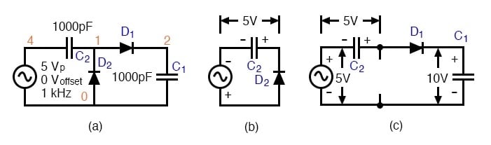
Figure 1. Half-wave voltage doubler (a) is composed of (b) a clamper and (c) a half-wave rectifier.
Half-wave Voltage Doubler Operation Circuit Analysis
Referring to Figure 1(b) above , C2 charges to 5 V (4.3 V considering the diode drop) on the negative half cycle of AC input. The right end is grounded by the conducting D2. The left end is charged at the negative peak of the AC input. This is the operation of the clamper.
During the positive half cycle, the half-wave rectifier is shown in Figure 1 (c) above . Diode D2 is out of the circuit since it is reverse-biased. C2 is now in series with the voltage source. Note the polarities of the generator and C2, series aiding. Thus, rectifier D1 sees a total of 10 V at the peak of the sinewave, 5 V from the generator, and 5 V from C2. D1 conducts waveform v(1), as illustrated in Figure 2, charging C1 to the peak of the sine wave riding on 5 V DC - Figure 2 v(2). Waveform v(2) is the output of the doubler, which stabilizes at 10 V (8.6 V with diode drops) after a few cycles of sine wave input.
|
|
*SPICE 03255.eps C1 2 0 1000p D1 1 2 diode C2 4 1 1000p D2 0 1 diode V1 4 0 SIN(0 5 1k) .model diode d .tran 0.01m 5m .end |
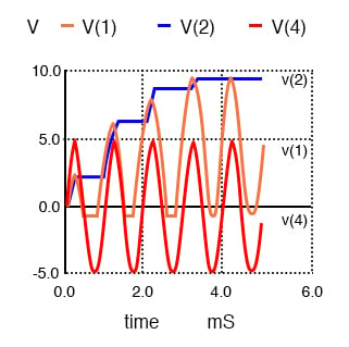
Figure 2. Voltage doubler: v(4) input. v(1) clamper stage. v(2) half-wave rectifier stage, which is the doubler output.
Full-Wave Voltage Doubler
The full-wave voltage doubler is composed of a pair of series stacked half-wave rectifiers (Figure 3). The corresponding netlist is in Figure below.
Full-Wave Voltage Doubler Operation Analysis
The bottom rectifier charges C1 on the negative half cycle of input. The top rectifier charges C2 on the positive half-cycle. Each capacitor takes on a charge of 5 V (4.3 V considering diode drop). The output at node 5 is the series total of C1 + C2 or 10 V (8.6 V with diode drops).
|
|
*SPICE 03273.eps D1 0 2 diode D2 2 5 diode C1 3 0 1000p C2 5 3 1000p V1 2 3 SIN(0 5 1k) .model diode d .tran 0.01m 5m .end |
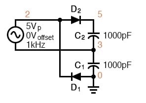
Figure 3. Full-wave voltage doubler consists of two half-wave rectifiers operating on alternating polarities.
Note that the output v(5) in Figure 4 reaches full value within one cycle of the input v(2) excursion.
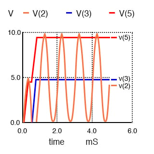
Figure 4. Full-wave voltage doubler: v(2) input, v(3)voltage at mid point, v(5) voltage at output.
Deriving Full-wave Doublers from Half-wave Rectifiers
The figure below illustrates the derivation of the full-wave doubler from a pair of opposite polarity half-wave rectifiers (a). The negative rectifier of the pair is redrawn for clarity (b). Both are combined at (c), sharing the same ground. At (d), the negative rectifier is re-wired to share one voltage source with the positive rectifier. This yields a ±5 V (4.3 V with diode drop) power supply, though 10 V is measurable between the two outputs. The ground reference point is moved so that +10 V is available with respect to the ground.
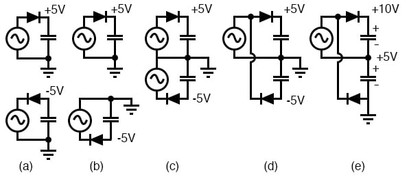
Figure 5. Full-wave doubler: (a) Pair of doublers, (b) redrawn, (c) sharing the ground, (d) sharing the same voltage source. (e) move the ground point.
Voltage Tripler
A voltage tripler (Figure 6 below) is built from a combination of a doubler and a half-wave rectifier (C3, D3). The half-wave rectifier produces 5 V (4.3 V) at node 3. The doubler provides another 10 V (8.4 V) between nodes 2 and 3, for a total of 15 V (12.9 V) at the output node 2 with respect to ground.
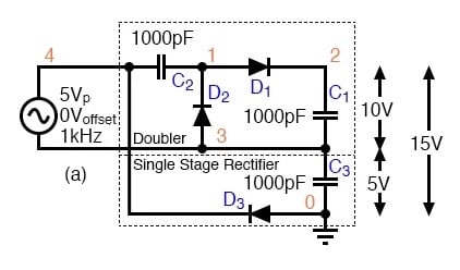
Figure 6. Voltage tripler composed of doubler stacked atop a single stage rectifier.
Note that V(3) in Figure 7 rises to 5 V (4.3 V) on the first negative half cycle. Input v(4) is shifted upward by 5 V (4.3 V) due to 5 V from the half-wave rectifier. And 5 V more at v(1) due to the clamper (C2, D2). D1 charges C1 (waveform v(2)) to the peak value of v(1). The netlist for the schematic of Figure 6 is also included in Figure 7.
|
|
*SPICE 03283.eps C3 3 0 1000p D3 0 4 diode C1 2 3 1000p D1 1 2 diode C2 4 1 1000p D2 3 1 diode V1 4 3 SIN(0 5 1k) .model diode d .tran 0.01m 5m .end |
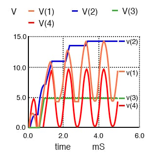
Figure 7. Voltage tripler: v(3) half-wave rectifier, v(4) input+ 5 V, v(1) clamper, v(2) final output.
Voltage Quadrupler
A voltage quadrupler is a stacked combination of two doublers shown in Figure 8. Each doubler provides 10 V (8.6 V) for a series total at node 2 with respect to ground of 20 V (17.2 V)
Figure 8. Voltage quadrupler, composed of two doublers stacked in series, with output at node 2.
The waveforms of the quadrupler are shown in Figure 9. Two DC outputs are available: v(3), the doubler output, and v(2), the quadrupler's output. Some of the intermediate voltages at clampers illustrate that the input sinewave (not shown), which swings by 5 V, is successively clamped at higher levels: at v(5), v(4), and v(1). Strictly v(4) is not a clamper output. It is simply the AC voltage source in series with the v(3) doubler's output. Nonetheless, v(1) is a clamped version of v(4).
|
|
*SPICE 03441.eps C22 4 5 1000p C11 3 0 1000p D11 0 5 diode D22 5 3 diode C1 2 3 1000p D1 1 2 diode C2 4 1 1000p D2 3 1 diode V1 4 3 SIN(0 5 1k) .model diode d .tran 0.01m 5m .end |
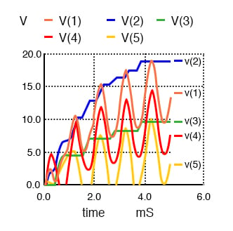
Figure 9. Voltage quadrupler: DC voltage available at v(3) and v(2). Intermediate waveforms: Clampers: v(5), v(4), v(1).
Notes on Voltage Multipliers and Line-driven Power Supplies
Some notes on voltage multipliers are in order at this point. The circuit parameters used in the examples (V = 5 V 1 kHz, C = 1000 pf) do not provide much current, microamps. Furthermore, load resistors have been omitted. Loading reduces the voltages from those shown. If the circuits are to be driven by a kHz source at low voltage, as in the examples, the capacitors are usually 0.1 to 1.0 µF, so milliamps of current are available at the output. If the multipliers are driven from 50/60 Hz, the capacitor is a few hundred to a few thousand microfarads to provide hundreds of milliamps of output current. If driven from line voltage, pay attention to the polarity and voltage ratings of the capacitors.
Finally, any direct line-driven power supply (no transformer) is dangerous to the experimenter and line-operated test equipment. Commercial direct-driven supplies are safe because the hazardous circuitry is enclosed to protect the user. When breadboarding these circuits with electrolytic capacitors of any voltage, the capacitors will explode if the polarity is reversed. Such circuits should be powered up behind a safety shield.
Cockcroft-Walton Multiplier
A voltage multiplier of cascaded half-wave doublers of arbitrary length is known as a Cockcroft-Walton multiplier, as illustrated in Figure 10. This multiplier is used when a high voltage at a low current is required. The advantage over a conventional supply is that an expensive high-voltage transformer is not required– at least not as high as the output.
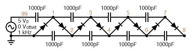
Figure 10. Cockcroft-Walton x8 voltage multiplier; output at v(8).
The pair of diodes and capacitors to the left of nodes 1 and 2 in Figure 10 constitute a half-wave doubler. Rotating the diodes by 45o counterclockwise and the bottom capacitor by 90o makes it look like Figure prior (a). Four of the doubler sections are cascaded to the right for a theoretical x8 multiplication factor. Node 1 has a clamper waveform (not shown), a sinewave shifted up by 1x (5 V). The other odd-numbered nodes are sinewaves clamped to successively higher voltages. Node 2, the output of the first doubler, is a 2x DC voltage v(2) in Figure 11. Successive even numbered nodes charge to successively higher voltages: v(4), v(6), v(8).
|
|
D1 7 8 diode C1 8 6 1000p D2 6 7 diode C2 5 7 1000p D3 5 6 diode C3 4 6 1000p D4 4 5 diode C4 3 5 1000p D5 3 4 diode C5 2 4 1000p D6 2 3 diode D7 1 2 diode C6 1 3 1000p C7 2 0 1000p C8 99 1 1000p D8 0 1 diode V1 99 0 SIN(0 5 1k) .model diode d .tran 0.01m 50m .end |
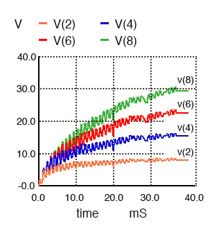
Figure 11. Cockcroft-Walton (x8) waveforms. Output is v(8).
Without diode drops, each doubler yields 2Vin or 10 V, considering two diode drops (10-1.4) = 8.6 V is realistic. For a total of 4 doublers, one expects 4·8.6 = 34.4 V out of 40 V.
Consulting Figure 10, v(2) is about right; however, v(8) is < 30 V instead of the anticipated 34.4 V. The bane of the Cockcroft-Walton multiplier is that each additional stage adds less than the previous stage. Thus, a practical limit to the number of stages exists. It is possible to overcome this limitation with a modification to the basic circuit. [ABR] Also note the time scale of 40 ms compared with 5 ms for previous circuits. It required 40 msec for the voltages to rise to a terminal value for this circuit. The netlist in Figure 11 above has a “.tran 0.010 m 50 m” command to extend the simulation time to 50 ms, though only 40 ms is plotted.
The Cockcroft-Walton multiplier serves as a more efficient high voltage source for photomultiplier tubes requiring up to 2000 V. [ABR] Moreover, the tube has numerous dynodes, terminals requiring connection to the lower voltage “even numbered” nodes. The series string of multiplier taps replaces a heat-generating resistive voltage divider of previous designs.
An AC line-operated Cockcroft-Walton multiplier provides high voltage to “ion generators” for neutralizing electrostatic charge and for air purifiers.
Voltage Multiplier Review
- A voltage multiplier produces a DC multiple (2,3,4, etc) of the AC peak input voltage.
- The most basic multiplier is a half-wave doubler.
- The full-wave double is a superior circuit as a doubler.
- A tripler is a half-wave doubler and a conventional rectifier stage (peak detector).
- A quadrupler is a pair of half-wave doublers
- A long string of half-wave doublers is known as a Cockcroft-Walton multiplier.
Related Content
Worksheets:


Can I get 220v from 5v input using cockcroft Walton multiplier?
Or else to 240v 50/60Hz output from 12v or 24v input?
Great Explanation ! I found it very useful and self explanatory.
But I would like to point out that in the Voltage Tripler Circuit, I guess D1 and D3 should be reversed. If D1 won’t be reversed, the output across C1 would be effectively zero. And then consecutively, D3 needs to be reversed otherwise the voltages across C1 and C3 will tend to cancel each other.
Thanks !