Facebook
 Google
 GitHub
 Linkedin
Discrete Semiconductor Devices and Circuits
BJT Amplifier Troubleshooting
11 questions By Tony R. Kuphaldt
-
Question 4 of 11
The three-stage amplifier shown here has a problem. Despite being supplied with good, “clean” DC power and an adequate input signal to amplify, there is no output signal whatsoever:

Explain how you would use the “divide and conquer” or “divide by two” strategy of troubleshooting to locate the amplification stage where the fault is. (This is where you divide the signal path into different sections, then test for good signal at points along that path so as to narrow the problem down to one-half of the circuit, then to one-quarter of the circuit, etc.)
Show the lines of demarcation where you would divide the circuit into distinct sections, and identify input and output test points for each of those sections.
Reveal answer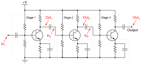
Challenge question: how well do you suppose this same troubleshooting strategy would work to locate the fault within a particular amplification stage?
Notes:Multi-stage amplifier circuits lend themselves well to the “divide and conquer” strategy of troubleshooting, especially when the stages are as symmetrical as these.
-
Question 5 of 11
In order to successfully troubleshoot any electronic circuit to the component level, one must have a good understanding of each component’s function within the context of that circuit. Transistor amplifiers are no exception to this rule. The following schematic shows a simple, two-stage audio amplifier circuit:

Identify the role of the following components in this audio amplifier circuit:
- The 0.47 μF capacitor connected to the microphone
- The 220 k Ω and 27 k Ω resistor pair
- The 4.7 μF electrolytic capacitor connected across the 1.5 k Ω resistor
- The 33 μF electrolytic capacitor connected to the speaker
- The 47 μF electrolytic capacitor connected to the power supply rail
Additionally, answer the following questions concerning the circuit’s design:
- What configuration is each stage (common-base, common-collector, common-emitter)?
- Why not just use one transistor stage to drive the speaker? Why is an additional stage necessary?
- What might happen if the 47 μF “decoupling” capacitor were not in the circuit?
- Why does the second stage of the amplifier not need its own voltage divider to set bias voltage as the first stage does?
Reveal answer- The 0.47 μF capacitor connected to the microphone: passes (AC) audio signal, blocks DC bias voltage from reaching microphone
- The 220 k Ω and 27 k Ω resistor pair: sets DC bias voltage for first transistor stage
- The 4.7 μF electrolytic capacitor connected across the 1.5 k Ω resistor: bypasses (AC) audio signal around emitter resistor, for maximum AC voltage gain
- The 33 μF electrolytic capacitor connected to the speaker: couples (AC) audio signal to speaker while blocking DC bias voltage from speaker
- The 47 μF electrolytic capacitor connected to the power supply rail: “decouples” any AC signal from the power supply, by providing a low-impedance (short) path to ground
The question regarding the necessity of the 47 μF decoupling capacitor is tricky to answer, so I’ll elaborate a bit here. Power supply decoupling is a good design practice, because it can ward off a wide range of problems. AC “ripple” voltage should never be present on the power supply “rail” conductors, as transistor circuits function best with pure DC power. The purpose of a decoupling capacitor is to subdue any ripple, whatever its source, by acting as a low-impedance “short” to ground for AC while not presenting any loading to the DC power.
Although it may not seem possible at first inspection, the lack of a decoupling capacitor in this audio amplifier circuit can actually lead to self-oscillation (where the amplifier becomes a tone generator) under certain power supply and load conditions! If the power supply is poorly regulated and/or poorly filtered, the presence of a decoupling capacitor will greatly diminish line-frequency “hum” noise heard in the speaker.
For the rest of the questions, I’ll let you figure out answers on your own!
Notes:Incidentally, this circuit makes a good “intercom” amplifier for a student project. Using a small dynamic speaker for the microphone, and another speaker (or audio headset) on the receiving end of a long cable connected to the amplifier output, students can easily talk between two rooms in a building, or even between buildings.
-
Question 6 of 11
Often times, component failures in transistor circuits will cause significant shifting of DC (quiescent) parameters. This is a benefit for the troubleshooter, as it means many faults may be located simply by measuring DC voltages (with no signal input) and comparing those voltages against what is expected. The most difficult part, though, is determining what DC voltage levels to expect at various points in an amplifier circuit.
Examine this two-stage audio amplifier circuit, and estimate the DC voltages at all the points marked by bold letters and arrows (A through G), with reference to ground. Assume that conducting PN junctions will drop 0.7 volts, that loading effects on the voltage divider are negligible, and that the transistor’s collector and emitter currents are virtually the same magnitude:
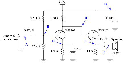
VA ≈
VB ≈
VC ≈
VD ≈
VE ≈
VF ≈
VG ≈
Reveal answerVA = 0 volts (precisely)
VB ≈ 0.98 volts
VC ≈ 0.28 volts
VD ≈ 7.1 volts
VE ≈ 6.4 volts
VF = 0 volts (precisely)
VG = 9 volts (precisely)
Follow-up question: explain why voltages VA, VF, and VG can be precisely known, while all the other DC voltages in this circuit are approximate. Why is this helpful to know when troubleshooting a faulted amplifier circuit?
Notes:The calculations used to estimate these values are quite simple, and should prove no trouble for students to derive who have a basic knowledge of DC circuit calculations (voltage dividers, series voltage drops, etc.).