
 Facebook
 Google
 GitHub
 Linkedin
Digital Circuits
Digital-to-Analog Conversion
13 questions By Tony R. Kuphaldt
-
Question 10 of 13
What is meant by the word resolution in reference to an ADC or a DAC? Why is resolution important to us, and how may it be calculated for any particular circuit knowing the number of binary bits?
Reveal answerThe resolution of either a digital-to-analog converter (DAC) or an analog-to-digital converter (ADC) is the measure of how finely its output may change between discrete, binary steps. For instance, an 8-bit DAC with an output voltage range of 0 to 10 volts will have a resolution of 39.22 mV.
Notes:Note that I did not hint how to calculate the resolution of a DAC or an ADC, I just gave the answer for a particular example. The goal here is for students to inductively “work backwards” from my example to a general mathematical statement about resolution.
There are actually two different ways to calculate the resolution, depending on the actual range of the converter circuit. For the answer given, I assumed that a digital value of 0x00 = 0.00 volts DC and that a digital value of 0xFF = 10.00 volts DC. If a student were to calculate the resolution for a circuit where 0xFF generated an output voltage just shy of 10.00 volts DC (e.g. an R-2R ladder network where Vref = 10 volts DC, and a full-scale binary input generates an output voltage just one step less than Vref), the correct answer for resolution would be 39.06 mV.
You may want to bring up such practical examples of resolution as the difference between a handheld digital multimeter and a lab-bench digital multimeter. The number of digits on the display is a sure clue to a substantial difference in ADC resolution.
-
Question 11 of 13
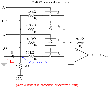
This digital-to-analog converter (DAC) circuit takes a four-bit binary input (input terminals A through D) and converts it to an analog voltage (Vout). Predict how the operation of this circuit will be affected as a result of the following faults. Consider each fault independently (i.e. one at a time, no multiple faults):
- Bilateral switch U1 fails open:
- Zener diode fails shorted:
- Solder bridge (short) past resistor R1:
- Resistor R6 fails open:
Reveal answer- Bilateral switch U1 fails open: Vout same for all odd numbered input conditions as it is for next lowest even-numbered input condition (e.g. input value of 5 gives same output as input value of 4).
- Zener diode fails shorted: Vout is nearly zero volts for any input condition.
- Solder bridge (short) past resistor R1: Vout saturates positive for any given odd-valued input condition.
- Resistor R6 fails open: Vout always saturated.
Follow-up question #1: is the arrow showing zener diode current drawn in the direction of electron flow or conventional flow?
Follow-up question #2: which input bit is the most significant (MSB) and which is the least significant (LSB)?
Notes:Questions like this help students hone their troubleshooting skills by forcing them to think through the consequences of each possibility. This is an essential step in troubleshooting, and it requires a firm understanding of circuit function.
-
Question 12 of 13
The following circuit generates an analog output voltage proportional to the value of the binary input, using pulse-width modulation (PWM) as an interim format. An eight-bit binary counter (CTR) continually counts in the üp” direction, while an 8-bit magnitude comparator (CMP) checks when the 8-bit binary input value matches the counter’s output value. The AND gate and inverter simply prevent the S-R latch from being “set” and “reset” simultaneously (when both A and B are maximum, both at a hex value of $FF), which would cause the output to be “invalid” when S and R were both active, and unpredictable when both S and R inputs returned to their inactive states:
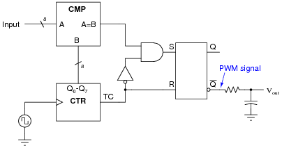
Explain how this circuit works, using timing diagrams if necessary to help show the PWM signal at \(\bar{Q}\) for different input values.
Reveal answerHere is a timing diagram to help get you started on a complete answer:
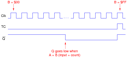
I’ll leave it to you to explain the relationship between the input value (A), the PWM duty cycle, and the analog output voltage.
Notes:This circuit provides students with an interesting exercise in timing analysis, as well as being a simple means of converting large binary values into analog output voltages without resorting to using large resistor networks.


