Facebook
 Google
 GitHub
 Linkedin
Discrete Semiconductor Devices and Circuits
Insulated Gate Field-Effect Transistors
39 questions By Tony R. Kuphaldt
-
Question 19 of 39
The “substrate” connection in a MOSFET is often internally connected to the source, like this:
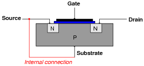
This turns the MOSFET from a four-terminal device into a three-terminal device, making it easier to use. One consequence of this internal connection, though, is the creation of a parasitic diode between the source and drain terminals: a PN junction that exists whether we want it to or not.
Add this parasitic diode to the MOSFET symbol shown here (representing the MOSFET cross-section shown above), and explain how its presence affects the transistor’s use in a real circuit:

Reveal answer
Follow-up question: how does the presence of this parasitic diode allow us to positively distinguish the source terminal from the gate terminal when identifying the terminals of a MOSFET with a multimeter?
Notes:The presence of this diode is a very important concept for students to grasp, as it makes the MOSFET a unilateral device for most practical purposes. Discuss the significance of this diode, and contrast the characteristics of a three-terminal MOSFET against the characteristics of a three-terminal JFET, which is a truly bilateral device.
-
Question 20 of 39
A technician is using a digital multimeter (with a “diode check” feature) to identify the terminals of a power MOSFET:
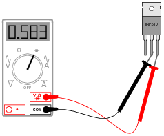
The technician obtains the following “diode check” voltage measurements, in this order:
- Black lead on middle terminal, Red lead on right terminal = 0.583 volts (shown in illustration)
- Red lead on middle terminal, Black lead on right terminal = O.L. (open)
- Black lead on middle terminal, Red lead on left terminal = O.L. (open)
- Black lead on middle terminal, Red lead on right terminal = 0.001 volts
- Red lead on middle terminal, Black lead on right terminal = 0.001 volts
Explain why the fourth and fifth measurements are so different from the first and second, respectively, when they were taken between the same terminals on the MOSFET. Hint: this particular MOSFET is an N-channel, enhancement-type.
Reveal answerThe act of taking the third measurement enhanced the transistor into the on (saturated) state by means of the multimeter’s output voltage in the diode test mode. The MOSFET then remained in its on state for the fourth and fifth measurements.
Follow-up question: where would the meter have to be connected in order to force the MOSFET into is off (cutoff) state?
Notes:Field-effect transistors, by their very nature being voltage-activated devices with extremely high input impedance, are more difficult to identify than bipolar junction transistors because the meter’s output in the “diode check” mode is sufficient to activate and de-activate them. This question showcases a practical example of this (the values actually came from real-life testing of an IRF510 transistor!).
-
Question 21 of 39
An important consideration when working around circuits containing MOSFETs is electrostatic discharge, or ESD. Describe what this phenomenon is, and why it is an important consideration for MOSFET circuits.
Reveal answer“Electrostatic discharge” is the application of very high voltages to circuit components as a result of contact or proximity with an electrically charged body, such as a human being. The high voltages exhibited by static electricity are very damaging to MOSFETs. I’ll let you research why!
Notes:Be sure to ask students to explain the mechanism of transistor damage resulting from ESD, and to discuss the sheer magnitude of static voltages typically generated in dry-air conditions. If you have any microphotographs of IC damage from ESD, present a few of them during discussion time for your students’ viewing pleasure.