Facebook
 Google
 GitHub
 Linkedin
Discrete Semiconductor Devices and Circuits
Junction field-effect transistors (JFET)
43 questions By Tony R. Kuphaldt
-
Question 16 of 43
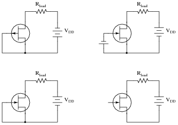
Identify each type of JFET (whether it is N-channel or P-channel), label the terminals, and determine whether the JFET in each of these circuits will be turned on or off:
Reveal answer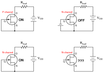
Follow-up question: explain why the lower-right circuit has question-marks next to the transistor. Why is the JFET’s state uncertain?
Notes:It is very important for your students to understand what factor(s) in a circuit force a JFET to turn on or off. Be sure to ask your students to explain their reasoning for each transistor’s status. What factor, or combination of factors, is necessary to turn a JFET on, versus off? One point of this question is to emphasize the non-importance of VDD‘s polarity when there is an external biasing voltage applied directly between gate and source.
-
Question 17 of 43
Identify each type of JFET (whether it is N-channel or P-channel), label the terminals, and determine whether the JFET in each of these circuits will be turned on or off:
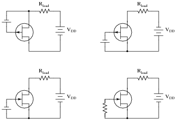
Additionally, identify which of these four circuits places unnecessary stress on the transistor. There is one circuit among these four where the transistor is operated in a state that might lead to premature failure.
Reveal answer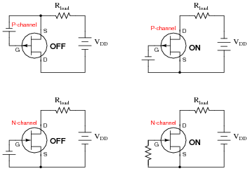
The upper-right circuit places unnecessary stress on the JFET.
Notes:It is very important for your students to understand what factor(s) in a circuit force a JFET to turn on or off. Be sure to ask your students to explain their reasoning for each transistor’s status. What factor, or combination of factors, is necessary to turn a JFET on, versus off? One point of this question is to emphasize the non-importance of VDD‘s polarity when there is an external biasing voltage applied directly between gate and source.
Discuss with your students precisely what is wrong with the upper-right JFET circuit. Why is the transistor being stressed? How do we avoid such a problem?
-
Question 18 of 43
When a reverse-bias voltage is applied between the gate and channel of a JFET, the depletion region within expands. The greater the reverse-bias voltage, the wider the depletion region becomes. With enough applied VGS, this expansion will cut off the JFET’s channel, preventing drain-source current:
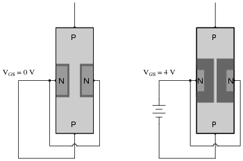
Something not immediately apparent about this effect is that the formation of a wide depletion region necessary for cut-off of a field-effect transistor is also affected by the drain-to-source voltage drop (VDS).
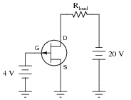
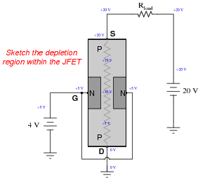
If we connect a gate-to-source voltage (VGS) large enough to force the transistor into cutoff mode, the JFET channel will act as a huge resistance. If we look carefully at the voltages measured with reference to ground, we will see that the width of the depletion region must vary within the JFET’s channel. Sketch this varying width, given the voltages shown in the illustration:
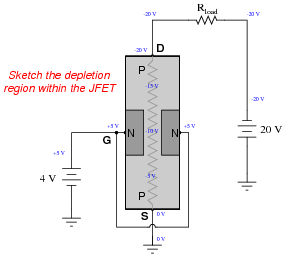
Something really interesting happens if we reverse the polarity of the 20 volt source: the relationship between drain and source changes, and so does the depletion region profile. Sketch the new varying width of the depletion region with the 20 volt source reversed, and comment on what you see:
Reveal answer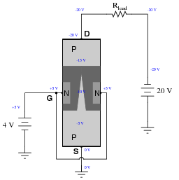
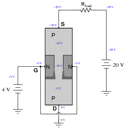
Follow-up question: you can see that the transistor doesn’t even cut off as expected with the 20 volt source reversed. What would we have to do to get this JFET to cut off with a only 4 volt control signal, since having reversed the 20 volt source?
Notes:There is more than one correct answer for the follow-up question. Discuss this with your students, emphasizing the importance of properly identifying drain and source according to VDS polarity.