Facebook
 Google
 GitHub
 Linkedin
Analog Integrated Circuits
Negative Feedback OpAmp Circuits
21 questions By Tony R. Kuphaldt
-
Question 19 of 21
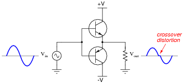
A complementary push-pull transistor amplifier built exactly as shown would perform rather poorly, exhibiting crossover distortion:
The simplest way to reduce or eliminate this distortion is by adding some bias voltage to each of the transistors’ inputs, so there will never be a period of time when the two transistors are simultaneously cutoff:
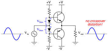
One problem with this solution is that just a little too much bias voltage will result in overheating of the transistors, as they simultaneously conduct current near the zero-crossing point of the AC signal. A more sophisticated method of mitigating crossover distortion is to use an opamp with negative feedback, like this:
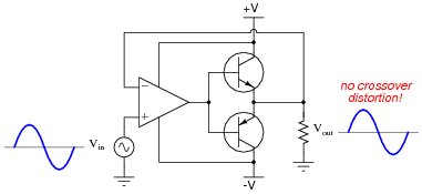
Explain how the opamp is able to eliminate crossover distortion in this push-pull amplifier circuit without the need for biasing.
Reveal answerBy sensing Vout, the opamp is able to “tell” whether or not the output voltage matches the input voltage, so it can drive the transistors as hard as they need to be driven to get the output voltage where it should be.
Challenge question: a more practical design blends the two strategies like this:

Explain why using less bias voltage and negative feedback with an opamp results in better performance than either method used alone.
Notes:Much could be said about good amplifier circuit design in this question, but the fundamental point is for students to see how negative feedback coupled with the extremely high gain of the opamp minimizes crossover distortion. Be sure to focus students’ attention on that point until they understand it well before launching into a discussion about the finer points of amplifier design.
It should be noted that this solution to crossover distortion in a push-pull amplifier circuit does not always yield the best results. In order for the opamp to ensure a smooth transition between half-cycles, its output must jump about 1.4 volts instantaneously to go from turning one transistor off to turning the other transistor on. Of course, no opamp can do this, because all have slew rate limitations. So, there will still be some crossover distortion, but not nearly as much as without the opamp (and with far less quiescent power dissipation that the two-diode solution!).
-
Question 20 of 21
The parasitic capacitance naturally existing in two-wire cables can cause problems when connected to high-impedance electronic devices. Take for instance certain biomedical probes used to detect electrochemical events in living tissue. Such probes may be modeled as voltage sources in series with resistances, those resistances usually being rather large due to the probes’ very small surface (contact) areas:
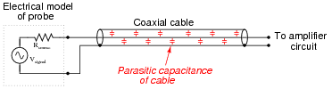
When connected to a cable with parasitic capacitance, a low-pass RC filter circuit is formed:
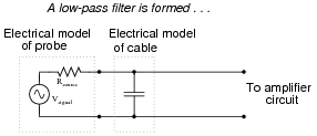
This low-pass filter (or passive integrator, if you wish) is purely unintentional. No one asked for it to be there, but it is there anyway just due to the natural resistance of the probe and the natural capacitance of the cable. Ideally, of course, we would like to be able to send the signal voltage (Vsignal) straight to the amplifier with no interference or filtering of any kind so we can see exactly what it is we’re trying to measure.
One clever way of practically eliminating the effects of cable capacitance is to encase the signal wire in its own shield, and then drive that shield with the exact same amount of voltage from a voltage follower at the other end of the cable. This is called guarding:
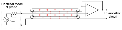
An equivalent schematic may make this technique more understandable:
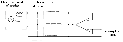
Explain why guarding the signal wire effectively eliminates the effects of the cable’s capacitance. Certainly the capacitance is still present, so how can it not have any effect on the weak signal any more?
Reveal answerThe guarding opamp holds the guard shield at the same potential as the center conductor, maintaining 0 volts across the parasitic capacitance between those two conductors. With no voltage across that capacitance, it might as well not even be there!
Follow-up question: although the center-to-guard capacitance may have zero volts across it at all times thanks to the opamp, the guard-to-(outer) shield capacitance still has the full signal voltage across it. Explain why this is of no concern to us, and why its presence does not form a low-pass filter as the original (unguarded) cable capacitance once did.
Notes:Guarding is a technique used in many test and measurement scenarios, and it serves as a great example of opamps used as voltage followers.
If students are not convinced of the seriousness of cable capacitance in an application such as the one described, suggest these values to them and ask them to calculate the cutoff frequency of the low-pass filter formed by Rsignal and Ccable:
- Rsignal = 20 MΩ
- Ccable = 175 pF
-
Question 21 of 21
Ideally, the input terminals of an operational amplifier conduct zero current, allowing us to simplify the analysis of many opamp circuits. However, in actuality there is a very small amount of current going through each of the input terminals of any opamp with BJT input circuitry. This may cause unexpected voltage errors in circuits.
Consider the following voltage buffer circuit:
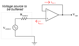
Ibias(−) does not cause any trouble for us, because it is completely supplied by the opamp’s output. The other bias current, though, does cause trouble, because it must go through the source’s Thévenin resistance. When it does, it drops some voltage across that intrinsic source resistance, skewing the amount of voltage actually seen at the non-inverting terminal of the opamp.
A common solution to this is to add another resistor to the circuit, like this:
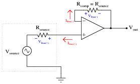
Explain why the addition of a resistor fixes the problem.
Reveal answerThe additional resistor should drop an equal amount of voltage, thus canceling out any bias voltage introduced by the bias current passing through the source’s internal resistance. Sizing this “compensating” resistor equal to the source’s Thévenin resistance assumes zero input offset current.
Notes:A simple voltage buffer circuit is the easiest context in which to understand the function of a bias current compensating resistor, and so it is presented here to allow students to see its impact.