Facebook
 Google
 GitHub
 Linkedin
Designing Around the USB-C Bottleneck: A Three-Diode ESD Protection Strategy
A USB 3.2 Gen 2x2 laptop port shows how matching TVS diode arrays to power, configuration, and data lines handles ESD without adding capacitance or board space.
Modern laptops route more through USB-C ports than any previous generation. Ports such as USB 3.2 Gen 2x2 Type-C combine up to 100 W of USB Power Delivery (PD) fast charging, 20 Gb/s SuperSpeed data, and DisplayPort or Thunderbolt alternate-mode video. All of it passes through the same connector.
Along with the power and data lines are the low-voltage configuration channel (CC) pins, which negotiate cable orientation, power contracts, and alt mode entry. The Sideband Use channel (SBU) pins carry sideband signaling for active alt modes. That convergence makes circuit protection more challenging.
A single electrostatic discharge event on the port can now threaten charging, configuration, data integrity, and video simultaneously. A leading laptop manufacturer designing USB 3.2 Gen 2x2 Type-C ports into its newest platform needed to protect its new communication port.
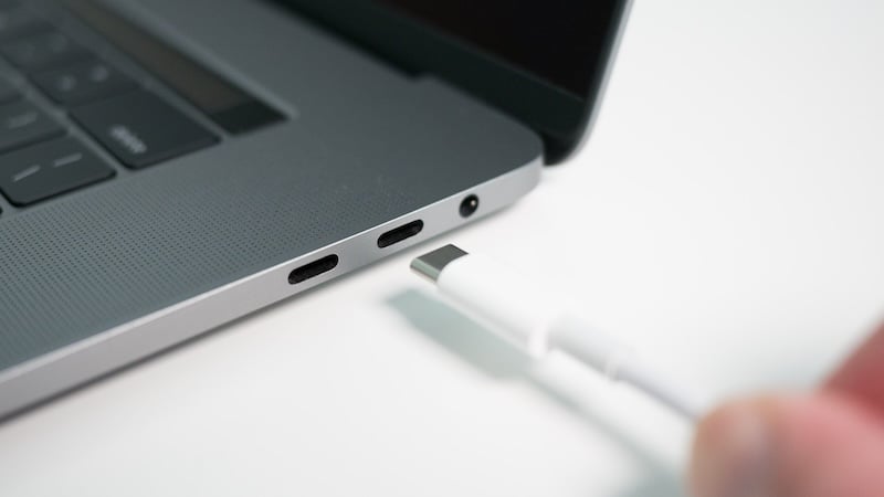
USB-C connectors are often repeatedly handled and exposed to ESD during normal use. Image used courtesy of Adobe Stock
Newer high-speed data specifications push more bandwidth through smaller, closer-packed pins. This narrows the design margin for board layout and component selection. Any ESD protection added to the port must clamp fast and at low voltage. It must also avoid adding capacitance that degrades high-speed signal performance and avoid consuming board space the platform cannot spare. Littelfuse worked with the manufacturer to protect its USB Type-C ports against ESD, surges, and other transients. The solution had to preserve signal integrity and take up no extra board space.
The Problem: Protecting High-Speed Ports Without Slowing Them Down
The design team needed to protect a USB 3.2 Gen 2x2 Type-C port carrying multiple high-speed protocols over the same connector. The project had these challenges:
- Signal integrity: any protection device added to the data lines needed capacitance low enough to avoid attenuating or distorting high-speed signals.
- ESD exposure: ports on a portable, frequently handled device face repeated contact and air-discharge events during normal use.
- Board space: laptop motherboards continue to shrink, leaving less room per port for protection circuitry.
- Multi-protocol complexity: a single USB-C port can carry USB data alongside video and other alternate-mode traffic, each with different transient-protection needs.
- Power delivery: USB PD Standard Power Range on this port supports up to 100 W (20 V at 5 A) on VBUS. A fault on the power line therefore risks overvoltage or overcurrent damage to charging circuitry, on top of the line’s own transient exposure.
The Root Cause: One Port, Multiple Transient Paths
Investigating the port design surfaced additional concerns:
- USB-C's ability to carry multiple protocols over one connector means a single port now has several distinct sets of lines. Each needs protection matched to its own speed and voltage profile.
- Repeated real-world handling exposes consumer ports to contact and air-discharge events, particularly in low-humidity conditions.
- The low-voltage CC and SBU configuration pins are especially sensitive to clamping voltage. They negotiate cable orientation and power contracts before any charging or data traffic begins.
- Tightly packed board layouts leave little room for large protection packages, pushing designers toward the smallest available footprints.
The Solution: Three Purpose-Built TVS Diode Arrays
Littelfuse recommended three SPA® TVS diode arrays, each matched to a different set of lines on the port.
All three sit directly behind the connector, where transients first enter the board, ahead of the port’s eFuses. These TVS diode arrays provide a fast response to transients, low clamping voltage, low capacitance, and low leakage current. All three device families ship in compact surface-mount packages. They are sized to fit the smaller board-space budget of modern laptop motherboards.
The system-level view of the USB-C port architecture below shows how VBUS, CC/SBU, and the SuperSpeed and USB 2.0 data lines route from the connector through the diode bank to the USB controller IC, with the eFuses and common-mode chokes positioned downstream of the protection devices.
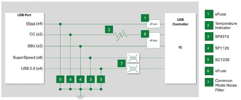
The protection diode bank sits directly behind the USB-C connector, ahead of the eFuses. Image used courtesy of Littelfuse.
Let's take a more detailed look at these three TVS diode arrays.
SC1230-01UTG
This 30 V unidirectional TVS diode designed to protect the port’s VBUS rail during USB PD 3.1 fast charging. Its 37 V typical clamping voltage keeps overvoltage events well below levels that could damage downstream charging ICs. A leakage current of just 0.02 μA (typical) at 30 V minimizes standby draw on the charging path. It safely absorbs ±30 kV contact or air discharge (IEC 61000-4-2) and dissipates 100 A of 8/20 μs surge current (IEC 61000-4-5). Four of these devices protect the port’s VBUS lines. The SC1230-01UTG comes in a 1.8 mm x 2.0 mm µDFN-6 package.
SP1120-01WTG
This device protects the CC and SBU pins. Its maximum capacitance of 50 pF leaves the configuration-channel signaling undisturbed. That signaling negotiates cable orientation, power contracts, and alternate-mode setup. It safely absorbs ±30 kV contact or air discharge (IEC 61000-4-2) without performance degradation. Four of these devices protect the port’s CC and SBU lines. The SP1120-01WTG has a 0.6 mm long flipchip footprint.
SP4315-01WTG
This 0.17 pF bidirectional TVS diode array is built for the port’s SuperSpeed data lines. A 7 V clamping voltage and deep snapback voltage keep it fast and precise enough to avoid distorting multi-gigabit signaling. It withstands a ±15 kV contact or air ESD discharge, exceeding IEC 61000-4-2 Level 4’s ±8 kV contact requirement. The TVS diode also protects against a 40 A electrical fast transient per IEC 61000-4-4. It also withstands 7 A of lightning surge per IEC 61000-4-5. Eight of these devices protect the port’s high-speed and Thunderbolt lines. SP4315-01WTG could also be a good choice for protecting the legacy USB 2.0 interfaces. This would provide a total of 12 placements to protect the data lines. The SP4315 adds bipolar protection and also has a 0.6 mm long flipchip footprint.
Integration Highlights: Placed at the Point of Entry
All the diode arrays, including four SC1230-01UTG, four SP1120-01WTGE, and twelve SP4315-01WTG, sit in a single cluster directly behind the USB-C receptacle, ahead of the port’s eFuses on the VBUS and CC lines. Transients are therefore clamped before they can reach the fusing and switching circuitry downstream. Grouping all three device families in one compact protection zone at the connector lets the design team route power, configuration, and high-speed traces in a compact pathway. Common-mode chokes filter high-frequency noise on the SuperSpeed and USB 2.0 lines. VBUS and CC eFuses sit behind the diode arrays in the signal path. The TVS devices absorb fast transients, while the eFuses handle sustained overcurrent conditions. Each protection element does the job for which it is optimized.
Results: Full-Port Protection, No Compromises
With all three SPA TVS diode arrays in place, the laptop manufacturer secured reliable protection on every USB-C line against ESD, EFT, and lightning-induced surges. The design adds no capacitance that could compromise data integrity and claims no board space the platform cannot spare. Testing confirmed that the laptop passed the IEC Standards. The port now supports the full range of a modern USB-C connection, including PD fast charging, configuration-channel negotiation, SuperSpeed data, and DisplayPort or Thunderbolt video. All of it is protected together in a single, compact design at the point where transients first enter the board.
For full electrical specifications, package dimensions, and test data behind this design, see the SC1230-01UTG TVS Diode, SP1120-01WTG TVS Diode Array, and the SP4315-01WTG TVS Diode Array datasheets.
Related Content