 Facebook
 Google
 GitHub
 Linkedin
How an Internal Faraday Shield and Small Ci-O Improve Optocoupler Galvanic Isolation
This article discusses how the use of three key design methods utilized in optocouplers improves galvanic isolation performance and presents an accompanying high voltage surge test as proof.
High voltage isolation in today’s context involves integrating subsystems with large voltage differences and systems ground potentials. This enables isolation for a wide variety of applications:
- Power supplies
- Motor control circuits of servo automation systems and industrial robots
- Battery management systems
- Photovoltaic (PV) inverters
- Electric vehicle (eV) inverters
- Ultra-fast and wireless charging stations to data communication
- Digital logic interface circuits
Basically, the most important components that provide the electrical isolation allowing for the integration of different subsystems by breaking direct conduction paths are called the isolators or couplers.
ICs can be combined into the isolators for various electrical functions including driving power electronic devices, high accuracy current and voltage measurements, analog and digital communications and logic interfaces, and isolated power supply conversions.
Types of Isolation Technology
There are three main types of isolator technologies, namely, optocoupler, magnetic coupler, and capacitive coupler. Table 1 below shows the key differences between the different isolation techniques, component safety certifications, and lifetime reliability failure mechanisms.
Table 1. Key Differences Between Different Isolation Techniques, Component Safety Certifications, and Lifetime Reliability Failure Mechanisms

The optocoupler transmits an electrical signal through the isolation barrier by converting the electrical signal to an optical signal using an LED. On the other side of the isolation barrier with a thickness of 0.08mm to 2mm, the LED converts the optical signal back to an electrical signal through the photodiodes. In terms of lifetime reliability, the integrity of an optocoupler's insulation material can be predicted by partial discharge measurement.
Theoretical dielectric strength values of insulation materials would always apply if optocoupler manufacturers could produce consistently pure insulation barriers. Often, however, high voltage dielectrics contain defects like voids and inclusions of air or other impurities. These voids will have lower breakdown strength than the surrounding dielectric and will discharge or arc when their breakdown strength is reached.
The discharge, however, is limited to the length of the void and after discharging, will slowly recharge with the limited current available through the good dielectric. The void eventually recharges to the breakdown voltage and discharges again. This process continues as long as the applied electric field remains high enough. These discharges are considered “partial” because they occur across the void in a limited portion of the length of the dielectric barrier. Partial discharges, which cannot be detected by leakage current measurements, can over time spread in the insulation, eventually leading to complete insulation breakdown. The problem then is to detect the presence of partial discharge during manufacturing tests in order to prevent this phenomenon from degrading devices in the field.
Key Design Methods of Broadcom Optocouplers
Broadcom optocouplers high voltage insulation strength is further enhanced with three key design methods. The first is by inserting a clear polyimide called Kapton tape in between the LED and photodiode. The second method is the use of a proprietary, low-cost Faraday shield which decouples the optocoupler input side from the output side. Figure 1 illustrates the isolation construction of Broadcom optocouplers.

Figure 1. Broadcom optocouplers isolation construction which incorporates Kapton tape and a Faraday shield for additional insulation strength.
The third method is by unique package design, optimized to minimize input-to-output capacitance, Ci-o. The importance of the three design methods will be discussed in detail in this technical paper with an accompanying high voltage surge test as proof.
A magnetic coupler uses two coils stacked on top of each other with a separating polyimide material of about 0.02mm in between. The application of an AC signal creates a magnetic field, which in turn induces an electric field in the secondary coil. Since the transmission is by magnetic field coupling, the magnetic coupler is also susceptible to nearby magnetic interference.
Figure 2 shows an example of magnetic coupler isolation construction with a single pair of top and bottom coils with polyimide insulation material in between the coils. To double the insulation strength, two sets of magnetic coils are used for one isolation path achieving an insulation thickness of about 0.04mm. The failure mode of the magnetic coupler insulation material is space charge degradation.

Figure 2. Magnetic coupler isolation construction with a single pair of top and bottom coils with polyimide insulation material in between.
The construction of a capacitive coupler is quite similar to a ceramic capacitor, whereby silicon dioxide (SiO2) dielectric with a thickness of about 0.015mm is sandwiched in between two metal plates, usually aluminum (Al), in close proximity. The SiO2 crystal is grown on top of the Al plate. The transmission of a signal through the capacitive isolation barrier is usually an AC electrical signal.
One of the factors that may affect the insulation strength of the capacitive coupler is how well the SiO2 crystal is grown. Defects in the crystal will weaken the insulation material. The lifetime reliability failure mode for the capacitive coupler is termed time-dependent dielectric breakdown (TDDB). Similar to a magnetic coupler, to double the insulation strength, two sets of capacitors are used for one isolation path and the insulation thickness is doubled to about 0.03mm. Figure 3 shows a typical double capacitor isolation construction.

Figure 3. Capacitive coupler isolation construction with two series caps where SiO2 dielectric is sandwiched in between by two Alu metal layers.
Optocouplers are certified to the component safety certification IEC 60747-5-5 for reinforced isolation. This international certification recognizes partial discharge as the failure mechanism for insulation material breakdown. As such, the certification only applies to optocouplers. The alternative isolation technologies like the magnetic and capacitive are certified German standard VDE 0884-10/11. Though the insulation material strength is determined by a partial discharge test, this may not be suitable to predict the lifetime reliability of the magnetic (space charge degradation) and capacitive couplers (TDDB).
High Voltage Surge Testing
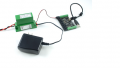
A quick bench test setup can be easily assembled to compare the insulation strength of various isolators. Figure 4 shows the test setup where the high voltage surge is applied using an ESD gun.

Figure 4. High voltage surge test setup is shown on the left and on the right side, the high voltage surge profile.
The voltage profile of the ESD gun has a very fast rise time of about 1ns and slow fall time of 30ms. This surge profile is different from the IEC 60060-1 standard surge profile of 1.2µs / 50µs, but it is sufficient for the purpose of comparisons of high voltage strength of different isolation technologies.
Three random samples each from two optocoupler manufacturers, Broadcom and Isolator A, one magnetic coupler (Isolator B) and one capacitive coupler (Isolator C) were selected for this high voltage surge test. These isolators are high precision current sensing sigma-delta modulators with an internal clock generator built into an 8-pin stretched surface mount package outline (SSO8). The isolation withstands voltage, Viso of this type of SSO8 package is rated 5kVrms per minute and with creepage and clearance distance of minimum 8mm.
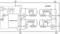
Figure 5 shows the schematic diagram of the PCB used to hold the device under test (DUT).

Figure 5. Schematic diagram of the PCB board used in the high voltage surge test.
Both isolated side power supplies were provided from 9V batteries separately and regulated down to 5V through an LDO voltage regulator on each side of the isolation. The test was carried out by applying a high voltage level starting at 15kV between Gnd1-Gnd2 of the sigma-delta modulators. The output clock and data signal were observed for any anomalies. If the outputs resumed normal functionality after the high voltage surge, voltage levels were increased by 1kV and the test continued up to 21kV test limit. If the output clock and/or data signal latched, the test would be stopped.
Utilizing a Faraday Shield
The high voltage surge will induce a high-density displacement current from Gnd1 to the input circuitry of the isolator and then transmit over to output circuitry and Gnd2 via capacitive structures or parasitic capacitance formed throughout the isolation barrier. Figure 6 below shows the various parasitic capacitance paths formed between the wire bonds of the input circuitry/input leadframe to the Faraday shield of Broadcom optocoupler.

Figure 6. Various parasitic capacitance paths formed between the wire bonds of the input circuitry/input leadframe to the Faraday shield of a Broadcom optocoupler. The Faraday shield is grounded to Gnd2 and helps to remove the displacement current.
The Faraday shield is grounded to Gnd2 and provides an electric and magnetic shielding to remove the displacement current. In capacitive or magnetic coupling solutions, the Faraday shield is not a viable solution. A Faraday shield would block the electric or magnetic fields used for data transmission in addition to transients.
Input-output Capacitance, Ci-o
In addition to the Faraday shield, Broadcom optocoupler leadframe and package design is optimized for smaller combined input to output capacitance, Ci-o. Table 2 shows the comparisons of Ci-o of various isolators.
Table 2. Input to Output Capacitance Comparisons Between Various Isolators

Displacement current follows the relation of i=c*dv/dt. With a smaller Ci-o, smaller displacement current is induced during the occurrence of a high voltage surge.
High Voltage Surge Test Results
Table 3 shows the results of a high voltage surge test on the isolators with different technologies.
Table 3. Results of the High Voltage Surge Test on Different Isolators

As evident from the test, Broadcom optocouplers remain robust against a high voltage surge whereby no failure is observed for all the units under the test up to a 21kV test limit. Isolator A (optocoupler) outputs permanently latched starting at 16kV onwards. Isolator B (magnetic coupler) outputs also latched from 16kV onwards but would recover once power on reset (p.o.r.) was carried out on either Vdd1, Vdd2 or both. For Isolator C (capacitive coupler), the outputs of the three units of Isolator C permanently latched at 15kV, 17kV and 21kV levels respectively. Although Isolator A, B, and C started to fail at about the same level, Isolator C recorded the widest range of the high voltage surge levels at which the test units failed.
Being an advocate for highly reliable optocouplers galvanic isolation technology, Broadcom’s portfolio includes internally clocked sigma-delta modulators for precision shunt-based current and voltage sensing solutions. Table 4 shows Broadcom product offerings of internally clocked sigma-delta modulators housed in the SSO8 package format.
Table 4. Broadcom's Internally Clocked Sigma-delta Modulators Housed in SSO8 Package Format

References
1. “Optocoupler Designer’s Guide”, Jan 3, 2014
2. “ACPL-C740 Optically Isolated Sigma-Delta Modulator”, ACPL-C740-DS103 Datasheet, Apr 01, 2019
3. “Ignore Detection of Partial Discharge Failures NOW--Pay Massive Amounts Later!”, Partial Discharge White Paper, Stephen Chaikin (Harris Tuvey)
4. “The ISO72x Family of High-Speed Digital Isolators”, Application Report, Kevin Gingerich and Chris Sterzik, Aug 2018
Related Content


not bad