Facebook
 Google
 GitHub
 Linkedin
Leaded Versus Leadless Packaging
Most components used in mass-produced small electronics come in leadless packages, but can elements of leaded packages be incorporated?
Most components used in mass-produced small electronics come in leadless packages, but can elements of leaded packages be incorporated?
Before we dive in, we should address a point of confusion. When referring to leaded and leadless packages, we are referring to whether or not a chip has metal leads (sometimes referred to as legs) that are mounted to circuit boards, not leaded versus leadless in terms of the element Lead.
Leaded and leadless packages have their own sets of strengths and weaknesses. By exploring their pros and cons, we can learn which are preferable for certain applications and even look to the future of component packaging.

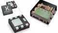
A PCB with a combination of leaded and leadless components
Advantages of Leadless Packaging
Ease of Use in Construction and Repair
Leaded packages have little legs around the perimeter of a component, which can either go through a PCB and are soldered on the PCB’s backside (through-hole) or directly to the PCB’s front side (surface mount).
Probably the most obvious advantage to leaded chip packages is that they’re easier to mount on PCBs. If you are prototyping and soldering components onto a PCB, yourself, they are more forgiving. They also make for PCBs that are easier to inspect and repair because you can see broken connections with the naked eye. Besides being smaller and less visible, leadless packages are more difficult to inspect because the contact points are under the chips. Usually, circuit boards with mostly leadless components are inspected and repaired with the help of X-ray machines.

A bus switch in a leaded package
DFM and Less Expensive Solder Pastes
Since the contact points on leaded packages are larger, they can use coarse solder paste, which is less expensive. Leadless components can be so small that the grains in coarse solder paste are almost as big as the components’ contact points, making them unable to connect.
Design for manufacturability (DFM) can be a crucial factor in the success of high-volume products. This can put designers in a quandary because, although most modern and mass produced devices use leadless packages, pins that are less than .4mm usually require type 4 solder paste and a step down mask for the manufacturing process. Both of these can greatly increase the cost of mass production.
Advantages of Leadless Packaging
Space Saving
While leaded packages are more forgiving when soldering prototypes manually, leadless packages have a plethora of advantages when it comes to manufacturing in mass quantities. Leadless packages save space by keeping the contact points underneath the component instead of on their perimeter. This extra space is crucial for applications like mobile devices, tablets, and wearables, where every millimeter counts. Devices like smartphones are made possible by leadless components.

A PicoGate in a leadless package
Ruggedness and Mechanical Strength
Another advantage of leadless components is their mechanical strength. In other words, they don’t separate from PCBs as easily. This is due to their high contact area to package ratio. Since the pins are on the bottom of the components instead of the perimeter, a larger portion of the component is attached to the PCB by solder. Leaded surface-mount components tend to lack the ruggedness of their through-hole and leaded counterparts.

Pulling and Shear force cause components to detach or lose connection with their PCBs. The more surface area on a package that is soldered to a PCB, the more likely it is to remain connected. You can learn more in this Leadless Package White Paper (PDF)
Can We Get the Best of Both?
People may not be soldering tiny leadless components in their garages anytime soon, but fortunately, most leadless components these days have some kind of evaluation board. By isolating the elements that make leaded and leadless packages great, we hope to help make mass-production more approachable by keeping costs down.
At Nexperia, we aim to incorporate the strengths of leaded packages into our leadless designs while maintaining the benefits of leadless packaging. For example, in our GX Packages for Discrete Logic, the pitches are all over .4mm while maintaining a small form factor.
If you’d like to learn more about designing for minimum footprint applications, Tom Wolf, a senior product application engineer at Nexperia will be hosting a free webinar on June 22nd at 9:00 AM Pacific Time.