
 Facebook
 Google
 GitHub
 Linkedin
Sustainable PCB Manufacturing: Eco-Friendly Materials and Practices
Current initiatives for sustainable PCB manufacturing often focus more on regulatory compliance than environmental responsibility. We will examine those initiatives plus newer ideas that could provide a better path forward for the PCB manufacturing industry.
In the modern landscape of electronics design and manufacture, sustainability has emerged as a critical challenge for engineers and the electrical engineering (EE) industry. Printed Circuit Boards (PCBs), integral components in virtually all electronic devices, face scrutiny for their environmental impact. The traditional PCB manufacturing process involves a range of toxic materials and generates significant waste, creating detrimental effects on both human health and the ecosystem.
The environmental cost of PCB manufacturing is multi-faceted. Key concerns include the use of hazardous materials like lead, brominated flame retardants (BFRs), and various solvents. Moreover, the disposal of electronics, often termed e-waste, results in heavy metals leaching into soil and water systems, leading to long-term ecological damage and health risks for nearby communities. With the global shift towards sustainability, engineers face immense pressure to devise eco-friendly alternatives for PCB manufacturing while maintaining cost-efficiency and performance standards.
Current Solutions and Their Limitations
Many current initiatives seek to address the sustainability challenge in PCB manufacturing, but they often fall short. The following subsections examine some of the prevalent approaches.
1. Lead-Free Solders
In response to regulatory prompts like the Restriction of Hazardous Substances Directive (RoHS) enforced in Europe and similar regulations worldwide, the shift towards lead-free solders has been one of the most visible changes in PCB manufacturing. Manufacturers have increasingly adopted alternatives such as SAC (tin-silver-copper) alloys.
While this transition effectively eliminates lead from PCBs—reducing the associated health risks of lead exposure—it introduces new challenges. For instance, the mining and extraction of silver and copper can have substantial environmental impacts, including habitat destruction, water pollution, and increased carbon emissions. Moreover, some of these alternative materials can have inefficiencies in solder joint reliability and thermal fatigue resistance.
2. Recycling Programs
The electronics industry is slowly recognizing the importance of recycling programs designed to recover valuable materials from end-of-life electronics. These programs help divert e-waste from landfills and recover metals like gold, silver, and copper. However, while recycling efforts can mitigate waste, they do not tackle the core issue of the materials used during the manufacturing cycle.
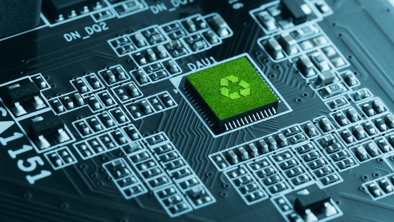
Recycling efforts are an important aspect of improving electronics sustainability. Image used courtesy of Adobe
The report from the Global E-waste Monitor 2024 by UNITAR estimates a drop in the documented collection and recycling rate from 22.3% in 2022 to 20% by 2030. This trend highlights a critical issue: without a comprehensive approach that emphasizes responsible sourcing and sustainable design practices, the industry's recycling initiatives may struggle to significantly impact the overall environmental challenges posed by electronic waste.
3. Halogen-Free Laminates
There has been a push for the adoption of halogen-free laminates as a means of reducing toxicity in PCBs. These alternatives are marketed as being safer for the environment and human health due to their reduced toxicity in case of fires. However, while halogen-free laminates reduce specific hazards, manufacturers often revert to using non-recyclable materials, leading to increased landfill waste. The trade-offs in heat resistance and mechanical performance compared to traditional laminates can also lead to lower reliability in high-performance applications—an essential consideration for engineers.
4. Chemical Treatment Technologies
Chemical treatments to mitigate the environmental impact of PCB manufacturing—like etching and cleaning agents—have been evaluated for their eco-friendliness. However, many conventional processes still rely extensively on harsh chemicals, contributing to air and water pollution. Engineers face difficulties in balancing the efficacy of these agents with their environmental footprint, as greener alternatives often come with high costs and longer processing times.
5. Technological Innovations
While some technological advancements in PCB manufacturing have emerged—such as the development of low-temperature soldering techniques and advanced circuit board designs that require fewer resources—the adoption of these technologies is often slow in ramping up. One major bottleneck is the need for significant investments in new machinery and training, making many small and medium enterprises hesitant to embrace these forward-thinking solutions.
6. Carbon Footprint and Energy Consumption
Manufacturing processes themselves are energy-intensive, leading to a substantial carbon footprint. The reliance on fossil fuels for energy continues to plague the industry, contributing to climate change. Though some companies are beginning to integrate renewable energy sources, the pace remains slow and often relies on substantial investments that smaller manufacturers may not afford.
7. Limited Awareness of Sustainability Practices
A further complication arises from the disparity in knowledge and engagement with sustainable practices across the industry. While larger corporations often have robust sustainability programs, smaller firms may lack the resources or expertise to implement similar initiatives. Without a comprehensive understanding of sustainability across the industry, the adoption of eco-friendly practices may remain inconsistent and uncoordinated.
8. Short-Term Focus
The electronics industry is, by nature, fast-paced, leading many manufacturers to prioritize rapid production and cost reduction over long-term sustainability. This short-term mindset undermines efforts to invest in sustainable materials and processes that may require upfront costs but promise long-term environmental benefits.
A Better Solution: Eco-Friendly Materials and Innovative Practices
While the initiatives described above represent strides toward sustainability, they oversimplify the problem and focus more on regulatory compliance rather than holistic environmental responsibility. The result is an ongoing reliance on processes and materials that still contribute to the degradation of our planet.
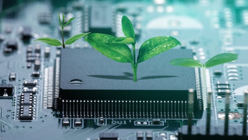
New efforts are needed to continue to improve PCB manufacturing. Image used courtesy of Adobe
Let’s take a closer look at four other initiatives that could provide a better path forward for the PCB manufacturing industry.
1. Bio-Based PCB Materials
One promising avenue is the development of eco-friendly, bio-based materials for PCB production. Recent advancements have led to the creation of substrates using organic, renewable resources, such as cellulose, lignin, and other natural polymers. These materials are biodegradable and environmentally benign, negating the need to rely on traditional, environmentally harmful components.
Additionally, bio-based resins are now being incorporated which offer excellent electrical properties similar to conventional epoxy resins. These materials can improve thermal stability while being less hazardous to manufacture, thus promoting a safer working environment.
2. Green Chemistry in Manufacturing
Another innovative approach involves the application of green chemistry principles to the PCB manufacturing process. This includes substituting hazardous solvents traditionally employed in PCB fabrication with more environmentally friendly options, such as water-based solutions or supercritical fluids. Such shifts reduce toxic byproducts and the overall ecological impact of the manufacturing process.
The implementation of advanced manufacturing processes, such as additive manufacturing (3D printing), is also gaining traction. This can significantly reduce material waste during the production cycle because components are built layer by layer rather than carved from larger blocks of material. 3D printing also allows for more complex geometries, which can lead to greater functionality while utilizing sustainable materials.
3. Circular Manufacturing Initiatives
Adopting a circular manufacturing model can further enhance sustainability. This approach focuses on creating closed-loop systems for materials. Engineers can design PCBs that are easier to disassemble after their lifecycle, facilitating the recovery of materials for reuse. By employing modular designs, components can be upgraded without needing to replace entire PCBs. This shift not only minimizes waste but also promotes longevity and reduces the demand for new raw materials.
Additionally, establishing partnerships with local recycling facilities can ensure that end-of-life PCBs are processed responsibly, creating a sustainable supply chain that benefits both manufacturers and the environment.
4. Life Cycle Assessment (LCA) Practices
The adoption of Lifecycle Assessment (LCA) is crucial for a better understanding of the environmental impacts associated with PCB manufacturing and disposal. LCA involves systematically evaluating the environmental effects of a product at every stage of its lifecycle—from raw material extraction to disposal. By employing LCA, engineers can identify areas of high environmental impact and pivot towards more sustainable practices.
A Greener Future for PCBs
Sustainable PCB manufacturing is at a critical juncture, challenged by the need to balance performance, cost, and environmental responsibility. Current solutions—while notable—often fail to address the root causes of ecological harm in electronics production. As engineers, it is vital to explore and adopt innovative materials, practices, and manufacturing strategies.
The transition to eco-friendly, bio-based materials, the integration of green chemistry, the adoption of circular manufacturing, and the implementation of Lifecycle Assessment represent a holistic strategy capable of transforming the PCB manufacturing landscape. Such measures can not only protect environmental integrity but also position the electronics industry as a leader in global sustainability efforts. By prioritizing sustainable practices in PCB manufacturing, the industry can pave the way for a greener future, ensuring that technological advancements do not come at the expense of our planet.







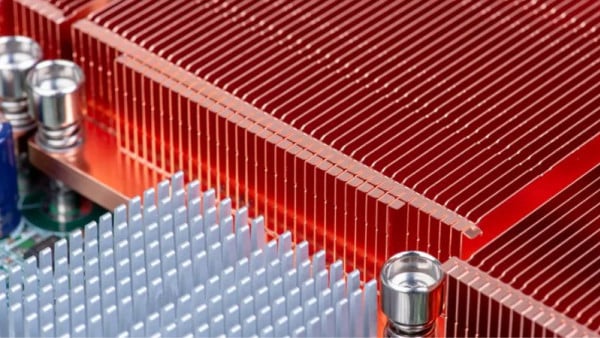





Sustainability often gets overlooked at the design stage, but it’s where some of the biggest gains can happen. Things like following fabrication standards can improve yields and cut waste significantly.
Summit Interconnect shared some insights on this at at IPC APEX EXPO 2025: https://summitinterconnect.com/blog/article/sustainability-in-pcb-design-insights-from-summit-interconnect-at-ipc-apex-expo-2025/