Facebook
 Google
 GitHub
 Linkedin
PCB Space Constraints? How Intermediate Bus Converters Can Help
Intermediate Bus Architecture is an emerging method that power designers are using to conserve PCB space. This article discusses the solution benefits and tradeoffs of adopting this technique, and how it may be scaled to address application-specific requirements.
The field of power electronics has become a well-established, highly researched industry dating back over 100 years to the invention of mercury-arc rectifiers in 1902 by Peter Cooper Hewitt. The invention of these rectifiers was followed by hot-cathode gas tube rectifiers in 1926, transistors in 1948, p-n-p-n silicon transistors in 1956, the IGBT in 1980, and many more. In the 21st century, power electronics continue to evolve in the fields of clean energy, electric vehicles, and server applications. Growth in these emerging industries requires power designers to find new and innovative solutions to meet evolving requirements calling for smaller, more cost-effective solutions.
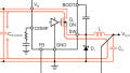
One such emerging architecture is the use of an Intermediate Bus Converter (IBC) in power applications. While the distributed power architecture (DPA) has become an industry standard for point of load (POL) designs, utilizing intermediate bus architecture (IBA) is an emerging method that enables designers to shrink solution size and use low-cost POL converters. POL converters are step-down DC-DC converters near the load, minimizing impedance and providing a precise voltage supply. They can be either power modules such as Intel® Enpirion® PowerSoCs, or discrete buck converters. Using IBA to power POL converters can often lead to lower costs and smaller solution sizes while maintaining competitive system efficiency.

Figure 1. One-stage traditional distributed power architecture vs. 2-stage intermediate bus architecture
The advantages of using IBA over DPA depends on the number of power rails converted, with more rails resulting in more space and cost savings. The system efficiency can remain competitive depending on the POL converters used.
Table 1. Comparison of IBA vs. DPA tradeoffs
| IBC Architecture | DPA Architecture | |
| Cost | Lower cost due to smaller inductors and POL converters | Higher cost due to higher voltage process technologies and inductance required |
| Efficiency | Lower system efficiencies due to power loss in 1st stage conversion | Higher system efficiencies in absence of intermediate stage |
| Solution Size | Smaller total solution size | Larger total solution size |
| Power Density | Higher power density solutions | Lower power density solutions |
| # of Rails | Ideal for use with > 3+ output rails | Ideal for use with < 3 output rails |
In the following discussion, the Intel EC2650QI 12-to-6 V Intermediate Bus Converter and Intel Enpirion PowerSoCs will be used as design examples.
Table 2. Intel Enpirion EC2650QI 12-to-6 V Intermediate Bus Converter
| Specifications | Features |
| VIN: 8 – 13.2 V | Up to 94% efficiency |
| VOUT: VIN /2 | 0.9 mm height |
| 6 A continuous output current | 36 W output power per bus converter |
| 150 mm² solution size | Parallel capable (up to four for 144 W total) |
Multi-Stage Power Conversion Approach Requiring Less PCB Space
When converting directly from 12 V in a 1-stage approach, the subsequent 12 V DC-DC power converters that are used require a 20 V or higher process technology to withstand the larger input. The higher voltage process is necessary to guarantee enough margin between operating range and device breakdown due to voltage spikes. The larger the voltage process, the larger the device, as more space is needed between the drain, source, and gate of the transistors inside.
In contrast, utilizing a 2-stage approach by first stepping down from 12 V to 6 V allows for lower input POL modules downstream. The lower input voltage modules are often smaller and competitively priced as they only require a 10 V process technology and do not need the internal circuitry to handle these higher input voltages.
Additionally, when converting from higher input voltages, the inductor must be able to handle the voltage difference during each switching cycle. When stepping down directly from 12 V, a higher inductance or higher switching frequency is required to minimize output ripple. Often, power designers choose to implement a higher inductance because higher switching frequency usually means more power loss and decreased efficiency. However, this higher inductance translates to more windings around the magnetic core of an inductor, which increases the inductor’s physical size. Using the IBC to step-down from 12 V to 6 V instead will allow designers to achieve similar ripple without the need to increase the inductor’s physical size of each POL.
Efficient Design Solutions Despite the Two-stage Conversion Penalty
Overall system efficiency in a 2-stage approach heavily relies on the bus converter’s efficiency. In order to avoid the common two-stage power conversion penalty, designers should choose a high efficiency IBC, such as the EC2650QI which delivers up to 94% conversion efficiency by using a switched capacitor topology.
For example:
In a 1-stage, direct conversion approach, converting 12 V to 3.3 V at 3 A could be 92% using the Intel EN2340QI.

Figure 2. Efficiency curve for the Intel Enpirion EN2340QI given a Vin of 12V.
In a 2-stage approach, converting 12 V to 6 V first could be 94% using the Intel EC2650QI.
- Then, converting 6 V to 3.3 V at 3 A could be 95% using the Intel EN6340QI.
- Finally, the total efficiency for the 2-stage approach would be: 0.94 x 0.95 = 89.3%.

Figure 3. Efficiency curve for the Intel Enpirion EC2650QI give a Vin of 12V.

Figure 4. Efficiency curve for the Intel Enpirion EN6340QI given a Vin of 5V.
In comparing 92% vs. 89.3%, we see the IBC creates some additional efficiency losses not present in a direct conversion approach. However, for some power designers or applications, the space savings gained may outweigh the compromises in efficiency.
This loss in efficiency can be further mitigated through several design choices, while still preserving the space savings gained from use of the IBC. Power designers may choose to specifically design the IBC on low current rails, which would minimize the additional wattage lost. They may also choose to select larger converters, which can make the overall design more efficient. Using the IBC enables engineers to scale their design choices to find an architecture that perfectly balances their size constraints, efficiency requirements, and cost needs.
When Should System Designers Choose to Design with IBA?
Generally, power designers should consider IBA when they have strict solution size or cost requirements, but some flexibility in efficiency. Particularly, using this 2-stage approach is often most beneficial when converting 3 or more rails, as the benefits of smaller solution size and lower cost become increasingly apparent. As stated above, an IBC architecture can be scaled and adapted to meet specific design requirements.
For example, if we use the Intel EN2342QI for the following four railings, the estimated system efficiency is approximately 87% with a total solution size of 800mm². If we use the IBC with four smaller POL converters, the estimated system efficiency is approximately 84% with a total solution size of 390mm². The 2-stage approach has a comparable efficiency while requiring less than half the PCB space, a 51% increase in space savings! With each additional railing, there is an average 100mm² in space savings, and more cost savings.

Figure 5. Example power trees for 1-stage vs. 2-stage IBC architecture using small POLs
Table 3. System-Level Comparison of Total Efficiency and Solution Size
| 1-Stage using Large POLs | 2-Stage using Small POLs |
| Efficiency: ~87% | Efficiency: ~84% |
| Total Solution Size: 800mm² | Total Solution Size: 390mm² |
For some designers, the drastic space and cost savings may compensate for the decrease in system efficiency. However, the efficiency can be further tuned and improved by substituting some small POL converters for larger ones, as in the following example.

Figure 6. Example power trees for 1-stage vs. 2-stage IBC architecture using small and large POLs
Table 4. System-Level Comparison of Total Efficiency and Solution Size
| 1-Stage using Large POLs | 2-Stage using Small & Large POLs |
| Efficiency: ~87% | Efficiency: ~85% |
| Total Solution Size: 800mm² | Total Solution Size: 590mm² |
In the above example, we substituted two of the small EN6340QI POL converters with the larger, more efficient EN6362QI converters. After doing so, the efficiency increased to over 85%, with a still 26% smaller solution size when compared to a DPA approach.
IBA Provides Additional Design Tools for Customized Solutions
In summary, IBA provides an additional design tool and unique opportunity for engineers to customize a solution that meets their specific needs. Incorporating the Intermediate Bus Converter allows power designers to use modules that require both a lower voltage process and inductance. These changes directly translate to smaller total solution sizes.
Any power lost from the additional stage can be mitigated by using a high-efficiency IBC and making application-specific design choices. One such example is the Intel Enpirion EC2650QI, which can be paralleled with up to four devices to create a 144 W bus, with each device requiring only 150 mm² in total solution size.
Additional Resources
- Intel Enpirion information page
- Introduction to Intel Enpirion Power Solutions Youtube video
- EC2650QI product page
- Intel EC2650QI Overview Youtube video
Related Content