Facebook
 Google
 GitHub
 Linkedin
On-Chip Diagnostic Features: A Single-Channel 16-Bit DAC from Analog Devices
In this article, we’ll take a look at the Analog Devices AD5758, which is a single-channel DAC with dynamic power control and HART connectivity.
In this article, we’ll take a look at the Analog Devices AD5758, which is a single-channel DAC with dynamic power control and HART connectivity.
In industrial automation and process control, we need digital-to-analog converters (DACs) that are capable of driving a wide range of loads. The AD5758 is a 16-bit DAC that can generate both current and voltage mode outputs for these industrial applications. I can say that the device actually combines an industrial current/voltage output driver, such as AD5750, with a general purpose DAC core that has many diagnostic features. This is done to facilitate design and diagnosis of typical industrial systems.
The AD5758 employs Dynamic Power Control (DPC) to minimize on-chip power dissipation. This power minimization, in turn, maximizes the temperature at which the device can safely operate. The AD5758 supports Highway-Addressable Remote Transducer (HART) connectivity. This is a protocol to communicate additional information over the legacy 4–20 mA analog instrumentation current loops (see this YouTube video for more information on HART). Additionally, the device includes several diagnostic features such as a watchdog timer, open/short circuit detection, SPI cyclic redundancy check, and an integrated analog-to-digital (ADC) converter to monitor several different parameters within the chip.
Let's take a look at the AD5758's datasheet.
Functional Block Diagram
The functional block diagram of the AD5758 is shown in Figure 1 below.
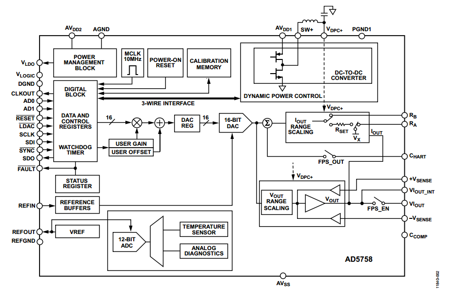
Figure 1. Image courtesy of Analog Devices.
In the rest of the article, we’ll take a look at some of the most important blocks illustrated in the above diagram.
What Is the Dynamic Power Control?
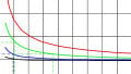
Dynamic power control (DPC) is a technique to minimize the on-chip power that’s dissipated in the output stage of a DAC. The technique is particularly useful in industrial systems where a DAC could be used to drive a wide range of loads. For example, assume that an ideal DAC must supply a current of up to 20 mA to a load that can vary from 100 $$\Omega$$ to 1 $$k \; \Omega$$. These two cases are illustrated in Figure 2.
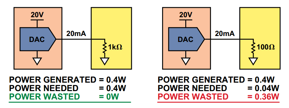
Figure 2. Image courtesy of Analog Devices.
Theoretically, we can find the minimum supply voltage of the system by finding the maximum voltage drop across the load which gives $$20 \; mA \times 1 k \; \Omega = 20 \; V$$. The supply voltage and the current supplied by the DAC output is the same for the two cases shown in the figure. Assume that our hypothetical DAC draws only as much as the current delivered to the load from the supply voltage. Hence, the power supply delivers a total power of $$V \times I=20 \; V \times 20 \; mA = 0.4 \; W$$ to the system.
How much of this total power is dissipated in the load and how much in the DAC itself? With a $$1-k \Omega$$ load, all of the power is delivered to the load. However, when the load is reduced to $$100 \; \Omega$$, the power dissipated in the load will be only $$0.04 \; W$$. Hence, $$0.4 \; W - 0.04 \; W = 0.36 \; W$$ will be dissipated in the DAC. As you can see, a small load can lead to a large on-chip power dissipation. This can increase the chip temperature to beyond the recommended levels.
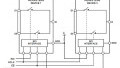
To minimize the on-chip power dissipation, the DPC technique dynamically reduces the supply voltage when the DAC is driving a small load. This is achieved by incorporating an on-chip DC-to-DC converter. The concept is illustrated in Figure 3.
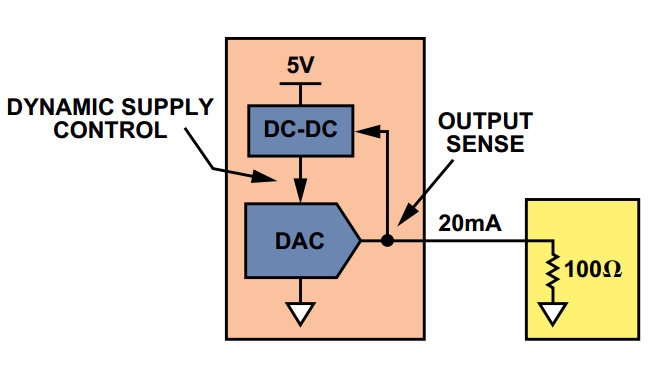
Figure 3. Image courtesy of Analog Devices.
As shown in Figure 4, only a few discrete components are required to operate the DC-to-DC converter of AD5758. In this figure, $$AV_{DD1}$$ is the supply for the DC-to-DC converter and $$V_{DPC+}$$ is the adjustable rail used to operate the DAC output buffers. As shown in the block diagram of Figure 1, $$V_{DPC+}$$ goes to both the current and voltage mode output circuitry.
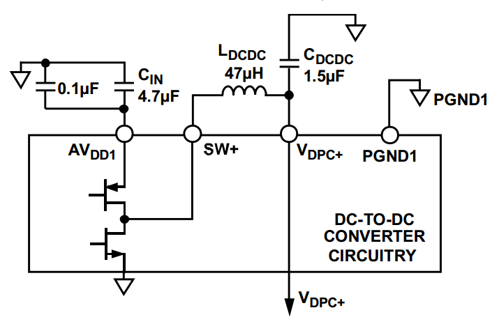
Figure 4. Image courtesy of Analog Devices.
Flexible Output Ranges
The AD5758 has a 16-bit DAC core which is depicted at the center of the block diagram in Figure 1. The output of this core can be converted to either a current or voltage signal at the $$VI_{OUT}$$ pin. Note that only one mode can be enabled at any one time. The device offers several programmable ranges for each of the current and voltage output modes. For example, some of the supported current ranges are 0 mA to 20 mA, 0 mA to 24 mA, 4 mA to 20 mA, 20 mA. There are also several ranges for the voltage output mode. Please refer to the datasheet for details. These programmable ranges allow us to deal with the variety of voltages and currents that an industrial system may need.
Current Output Mode
When the current output mode is selected, a voltage-to-current converter as shown in the diagram of Figure 5 is used.
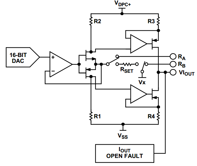
Figure 5. Image courtesy of Analog Devices.
Interestingly, the schematic shown in Figure 5 (and the voltage output circuitry that will be discussed later) are the same as those used in the AD5750 which is an industrial current/voltage output driver with programmable ranges. The block diagram of the AD5750 is shown in Figure 6.
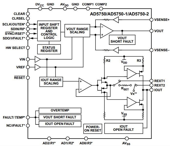
Figure 6. The block diagram of the AD5750. Image courtesy of Analog Devices.
As you can see, the AD5758 actually combines an industrial current/voltage output driver, i.e. AD5750, with a general purpose DAC and some other features that will be discussed in the rest of the article.
Note the two pins $$R_A$$ and $$R_B$$ in Figures 5 and 1. These two pins allow us to use an external current setting resistor instead of the internal $$R_{SET}$$. Using a low drift external resistor can improve the stability of the DAC output current over temperature variations.
Voltage Output Mode
The diagram for the voltage mode output is shown in Figure 7.
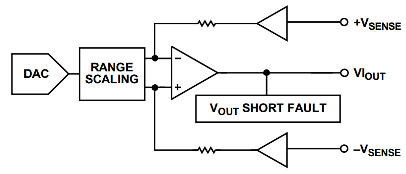
Figure 7. Image courtesy of Analog Devices.
As shown in this figure, in the voltage mode, the output of the core DAC is scaled and applied to the output buffers. The two inputs $$+V_{SENSE}$$ and $$-V_{SENSE}$$ are useful when remote sensing of a load is required. They allow us to predict and compensate for any voltage drops associated with a remote load. See page 36 of the datasheet for greater details.
The HART Connectivity
The AD5758 supports the HART communication protocol. The HART connectivity is provided by the $$C_{HART}$$ pin which is connected to the input of the current-mode buffers in Figure 1. What is the HART communication?
The HART protocol allows us to send both analog and digital signals on the same pair of wires. The analog signal which is a 4-mA to 20-mA current conveys the measured value of a process variable such as the output value of a pressure sensor. The digital signal is based on the Frequency-Shift Keying (FSK) modulation. It uses AC signals with 1200 Hz and 2200 Hz frequencies to represent a logic high and logic low, respectively. As shown in Figure 8, the digital signal is superimposed on the analog current signal.
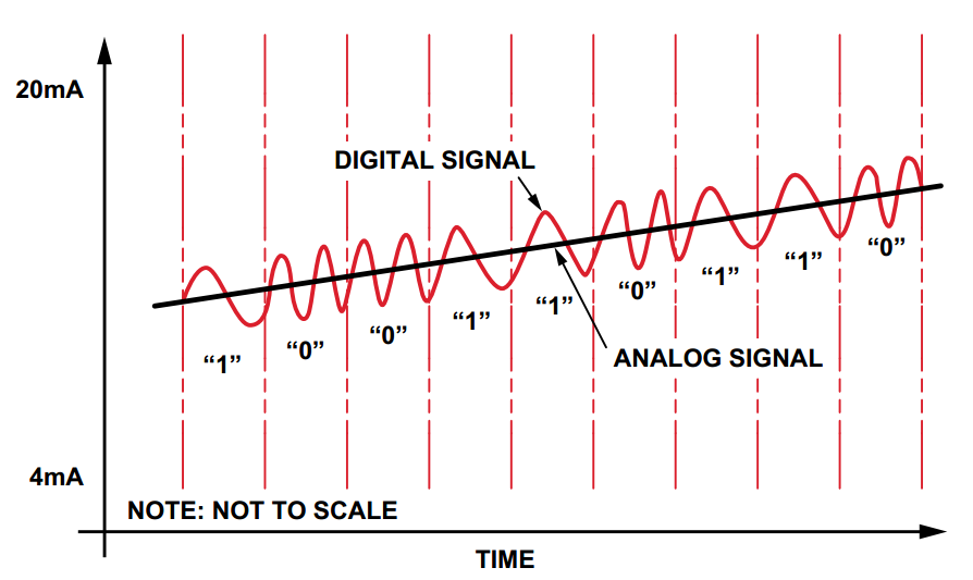
Figure 8. Image courtesy of Analog Devices.
The digital signal can be used to transmit various types of data such as a tagname, or calibration settings, or sensor diagnostics. See this YouTube video for more details about HART.
Diagnostic Features
The AD5758 includes several diagnostic features such as a watchdog timer, voltage output short-circuit protection, current output open-circuit detection, SPI cyclic redundancy check, etc. Refer to this Analog Devices document to read about using the watchdog timer to safely control the system when the communication between the system microcontroller and the AD5758 is lost.
In comparison with it predecessors, the AD5758 offers a wider range of diagnostic features. One of these new features is an integrated 12-bit diagnostic analog-to-digital converter (ADC) that can be used to monitor several different parameters within the chip. The input to this ADC is user selectable and can be parameters such as supplies, grounds, internal die temperatures, references, and external signals.
Evaluation Board
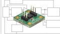
Analog Devices has developed an evaluation board for the AD5758 which is shown in Figure 9 below.
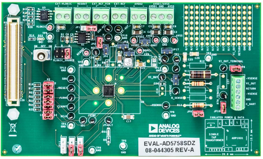
Figure 9. The evaluation board for the AD5758. Image courtesy of Analog Devices.
In this article, we looked at some of the most important features of the AD5758. If you have any experience with this industrial DAC or other similar parts, please let us know in the comments below.
Related Content