Facebook
 Google
 GitHub
 Linkedin
Picking Apart a New Switching Regulator from Analog Devices, the LT8361
This article will take a look at the Analog Devices LT8361, a low IQ switching regulator supporting boost, SEPIC, and inverting topologies.
This article will take a look at the Analog Devices LT8361, a low IQ switching regulator supporting boost, SEPIC, and inverting topologies.
The LT8361 is a switching regulator with an input voltage range of 2.8 V to 60 V. According to the LT8361 datasheet, it is best suited for the following applications:
- Industrial and automotive
- Telecom
- Medical diagnostic equipment
- Portable electronics
In “Burst Mode” configuration, the device is capable of operating with a quiescent current of 9 $$\mu A$$. It incorporates a rugged built-in power switch that supports output voltage and current values of 100 V and 2 A, respectively.
The LT8361 relies on a single feedback pin for both positive and negative outputs and uses spread spectrum frequency modulation (SSFM) to achieve a higher EMI performance.
In the following sections, we'll go over parts of the datasheet and discuss the device's most salient features and mechanisms.
Block Diagram
The block diagram of the LT8361 is shown in Figure 1 below.
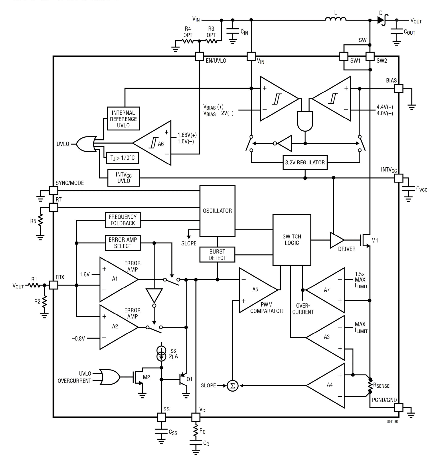
Figure 1. Image courtesy of Analog Devices. Click to enlarge.
Basic Boost Converter Operation
Let’s first review the basic idea behind a boost converter by replacing the LT8361 with a switch represented by M1 as shown in Figure 2 below.
Note that this model doesn’t include the feedback mechanism necessary to control the on-time of the switch. The feedback will be discussed in the next section.
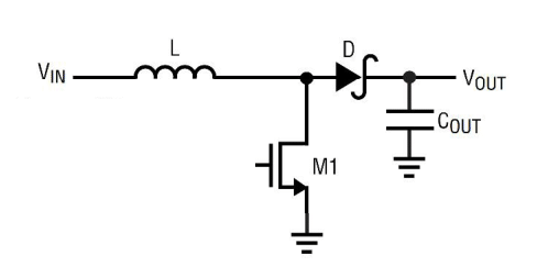
Figure 2. The schematic of a basic boost converter.
The goal of a boost converter is to develop and maintain a fixed output voltage, $$V_{OUT}$$, that is larger than the input voltage, $$V_{IN}$$.
The output voltages can be controlled by intermittently opening and closing the switch implemented by the M1 transistor in Figure 2. Note that the diode, D, prevents the load capacitor $$C_{OUT}$$ from being discharged through M1. So the converter circuitry will only charge this capacitor.
First, M1 is turned on and current flows through the inductor from input $$V_{IN}$$ to the ground. This act stores some energy in the inductor in the form of a magnetic field. Next, we open the switch. We know that the current through an inductor cannot change instantly; energy in the magnetic field creates a voltage that charges the capacitor. The value of the output voltage is determined by the current that’s forced to flow through the inductor.
How can we control the value of the inductor current? This can be done by controlling the on-time of the switch. If we keep the switch on for a long time, a very large current will flow through the inductor (inductors act as a short circuit when a DC voltage is applied to them for a long time). Hence, we can control the on-time of the switch to control the inductor current and consequently the output voltage.
Note that since the capacitor can be discharged by the load that will be connected to the output, we’ll have to periodically turn the switch on and charge the capacitor. Hence, we’ll need a feedback loop that periodically senses the output voltage and generates a pulse width modulated (PWM) signal to appropriately control the switch on-time. In this way, we can make sure that the capacitor voltage will remain fixed.
Now that we have a basic understanding of a boost converter, let’s take a look at the other parts of the block diagram in Figure 1.
Feedback Keeping the Output in Regulation
As we discussed above, a feedback loop is required to sense the output voltage and control the switch on-time accordingly. The main blocks of the feedback path of the LT8361 are shown in Figure 3.
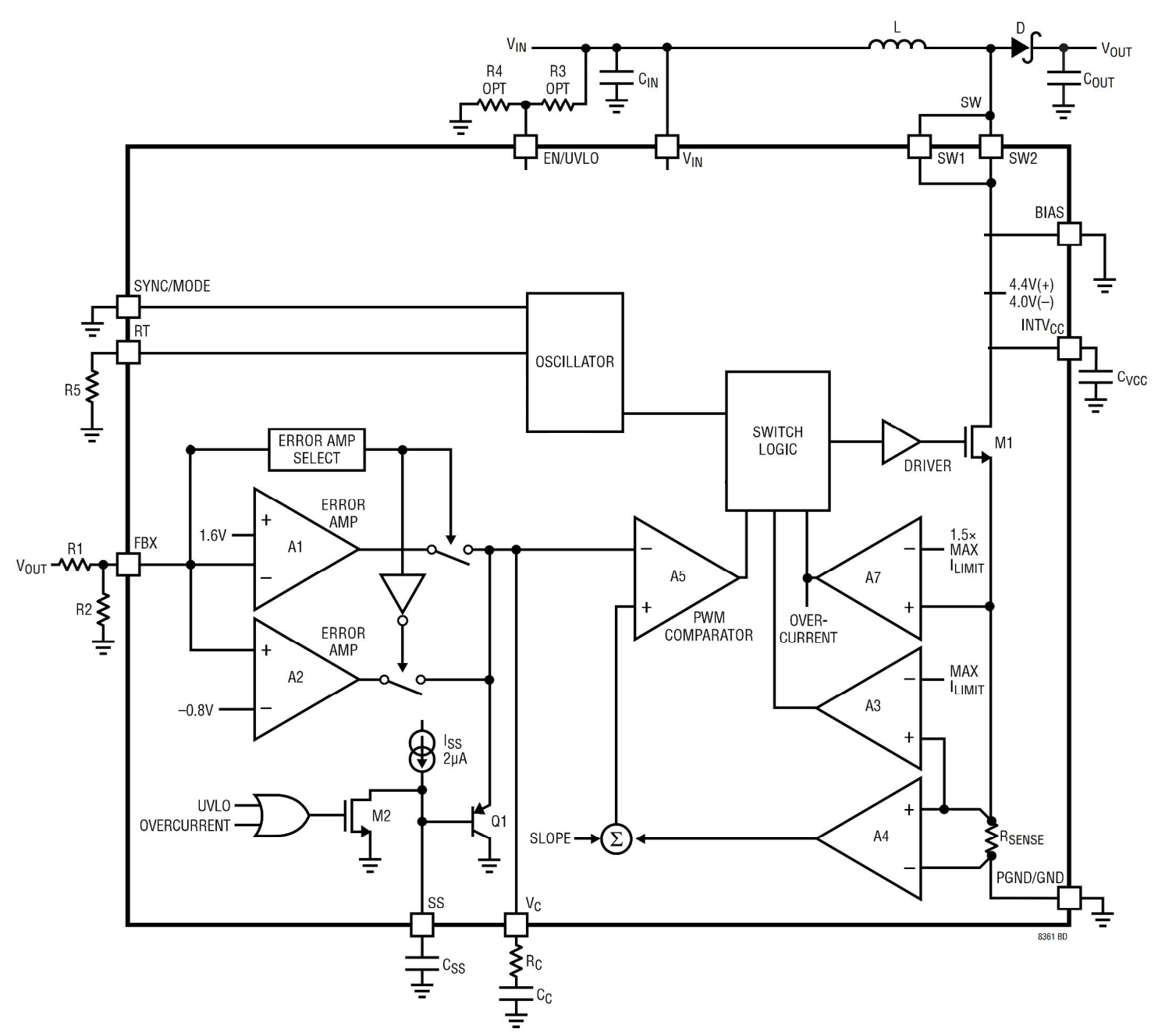
Figure 3. The important blocks in the feedback path of the LT8361. Click to enlarge.
As shown in this figure, the output $$V_{OUT}$$ is applied to a voltage divider created by R1 and R2. Hence, the voltage on the FBX pin is
$$V_{FBX}=\frac{R2}{R1+R2}\times V_{OUT}$$
Equation 1
This voltage is applied to two error amplifiers denoted by A1 and A2 in the figure. There is an “ERROR AMP SELECT” block that puts either A1 or A2 in the feedback path. The error amplifiers compare the voltage on the FBX pin with an internal reference voltage (1.60 V or -0.8 V depending on which error amplifier is chosen).
For now, assume that A1 is put in the feedback path. Therefore, $$V_{FBX}$$ given by Equation 1 will be compared with 1.60 V. As you may have guessed, the internal reference voltage is, in fact, our setpoint or desired value for the $$V_{FBX}$$. When $$V_{FBX}$$ becomes larger (smaller) than 1.60 V, A1 decreases (increases) the voltage of the $$V_C$$ pin.
There’s another comparator denoted by “PWM COMPARATOR”, A5, in Figure 3. This compares $$V_C$$ with the output of the A4 comparator (We are ignoring “SLOPE” for simplicity). The output of A4 is a voltage proportional to the current flowing through the switch (or equivalently proportional to the current flowing through the inductor when the switch is on). Note that the input of A4 is the voltage across the $$R_{SENSE}$$ resistor which is in series with the switch. Hence, A5 compares a voltage proportional to the inductor current with $$V_C$$. When the inductor current goes beyond a certain level, the “PWM COMPARATOR” trips and turns the power switch off.
If we use the A2 error amplifier, the setpoint for the FBX pin voltage will be -0.8 V and the converter will be in its inverting configuration.
Note the series resistor-capacitor network connected to the $$V_C$$ pin. This network performs compensation for the feedback loop. It affects the stability and the transient response of the system. We have to check the stability of the system for different operating conditions, such as different load currents and input voltages, in the entire temperature range of interest.
Refer to the device datasheet for details about choosing the appropriate values for the compensation network.
Frequency of Switching
The LT8361 uses an oscillator to determine the frequency of the PWM signal. The frequency of the oscillator, depicted at the center of the block diagram of Figure 3 above, can be programmed by connecting resistors of different values to the RT pin.
The oscillator frequency ranges from 300 kHz to 2 MHz depending on the value of the RT resistor. The datasheet gives the equation for finding the required resistor value for a given frequency of oscillation.
Internal Regulator
The LT8361 incorporates a low dropout linear regulator to provide a regulated 3.2-V supply for the internal loads of the chip. The linear regulator and its connection with the other blocks can be more easily observed in Figure 4.
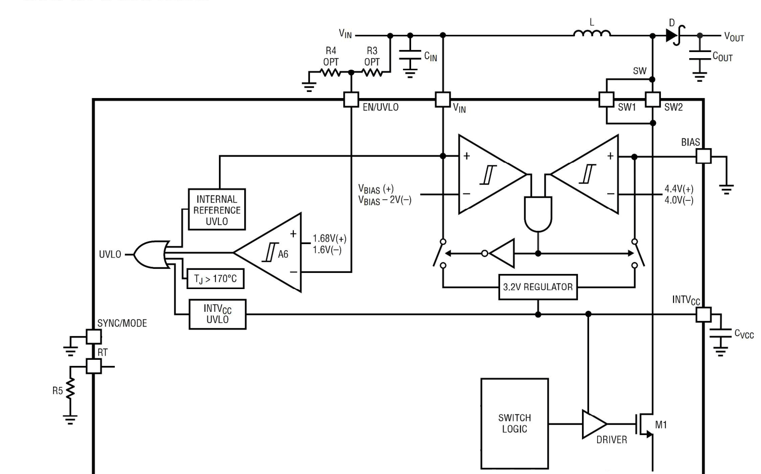
Figure 4. Click to enlarge.
The high transient currents drawn by the power MOSFET gate driver are supplied by the internal 3.2-V regulator. To this end, we’ll have to bypass the INTVCC pin with a 1-$$\mu F$$ low ESR capacitor to ground. Also, note that the 3.2-V regulator can draw its power from either the input $$V_{IN}$$ or the BIAS pin. Refer to the datasheet for more details.
Fault Protection
The LT8361 has several fault protection mechanism. For example, when the inductor current goes beyond a certain level the amplifier A7 sets the “OVERCURRENT” signal in Figure 3. This turns on the M2 transistor and the SS pin gets discharged. This will, in turn, pull down the $$V_C$$ pin through the Q1 transistor. Considering our discussion about the LT8361 feedback loop, we know that pulling down $$V_C$$ will prevent the power switch M1 from turning on (because a small current through the inductor will generate a positive voltage at the output of A4 and will force the “PWM COMPARATOR” to trip).
There are other fault protection mechanisms included in the LT8361. For example, as shown in Figure 1, an undervoltage condition on $$INTV_{CC}$$ pin and a thermal lockout where the junction temperature goes above 170 $$^{\circ} C$$ can set the UVLO signal. This will turn on the M2 transistor and ultimately will prevent the power switch from turning on in a way similar to the inductor overcurrent condition.
Burst Modes of Operation
When the LT8361 is connected to a light load, a smaller number of current pulses are required to keep the output in regulation. In such cases, we can use the device in its Burst mode of operation where the frequency of the current pulses decreases and each current pulse is followed by a sleep period. In the sleep periods, the device draws only 9 $$\mu A$$. That’s why the LT8361 can offer a higher light load efficiency. Figure 5 shows the Burst frequency versus the load current.
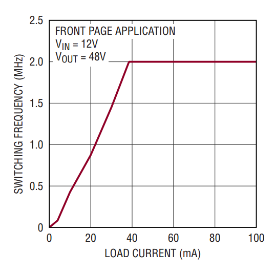
Figure 5. Image courtesy of Analog Devices.
As shown in this figure, for load currents below about 40 mA, reducing the load current leads to a decrease in the switching frequency. As the switching frequency decreases, the device will experience longer sleep periods.
EMI Performance
The LT8361 uses spread spectrum frequency modulation (SSFM) to achieve a higher EMI performance. Please refer to the datasheet for more information.
In this article, we looked at some of the most important features of the LT8361 from Analog Devices. If you have any experience with this switching regulator or other similar parts, please let us know in the comments below.