 Facebook
 Google
 GitHub
 Linkedin
Dialog Semiconductor Shrinks PSU Size with Zero Voltage Switching
Recently, Dialog released a new chipset which is said to reduce high power density power supply design by up to 50%. How does zero voltage switching play into it?
One of the biggest trends in power supply unit (PSU) design for consumer electronics is a push for faster and faster device charging. This pursuit has seen much success; however, engineers are left to work with devices exhibiting higher and higher power densities as they achieve faster charging.
This trend in power density has led to increased component temperatures causing reliability and potential safety issues. As this trend continues, it has gotten to the point where traditional DC-DC converting technologies are no longer efficient enough, thus causing engineers to search for improved conversion techniques.

A classification of different types of DC-DC converters. Image used courtesy of Salem et al
One of these techniques is Zero Voltage Switching (ZVS) and has greatly succeeded in increasing PSU. Recently, Dialog Semiconductor announced a new PSU chipset that claims to leverage ZVS technology to decrease PSU design size by up to 50%.
Switching Losses: Shortcomings of Conventional DC/DC Conversion
In most conventional non-isolated buck regulators, a significant source of inefficiency is switching losses.
Switching losses are from the simultaneous occurrence of high-current and voltage waveforms imposed on the MOSFET switch during on/off and off/on transitions. This switching is generally known as “hard switching," which occurs during the overlap between voltage and current when switching the MOSFET on and off.

The overlap between MOSFET VDS and Id during hard switching is a major source of inefficiency in DC/DC converters. Image used courtesy of Digikey
One approach to fix this issue is to increase the rate of change of both the current and the voltage. While this approach does work, it comes with an undesirable side effect: electromagnetic interference (EMI). This EMI could be prohibitive in many applications.
Zero Voltage Switching
One solution to this problem is zero voltage switching (ZVS), which minimizes and, generally, removes the current-voltage overlap.

Hard switching (left) vs ZVS (right). Image used courtesy of Mouser
ZVS works by using circuit techniques and intelligent driver control to bring VDS to zero before the MOSFET is turned on. By using this technique, switching losses can be eliminated as there is no crossover between VDS and IDS. On top of this, there is minimal EMI and switching noise during turn-on.

A buck regulator with ZVS implementation. Image used courtesy of DigiKey
The ZVS buck regulator, shown above, first turns Q1 on at zero current and zero VDS. As current flows through Q1, energy is stored in the inductor and charge on the capacitor. Next, Q1 turns off, and Q2 turns on.
During this phase, the energy stored in the output inductor is delivered to the load and capacitor. Q2 stays on a little past the point where the inductor current reaches zero, pulling some energy from the capacitor and storing it in the output inductor.
Once this happens, Q2 is turned off, and the clamp switch turns on, clamping the VS node to Vout, which effectively isolates the inductor's current from the output. The switch then opens, and the inductor's energy resonates with the output capacitances of Q1 and Q2 in parallel. This behavior and subsequent discharging and charging of output capacitances allow Q1 to turn on again with a VDS equal to zero.
Dialog’s New Product
Now that the basics of ZVS have been covered, this article will look at a recent application using ZVS: Dialog Semiconductor's chipset for high-density AC/DC power supplies.
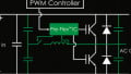
The chipset includes the iW9801 and iW9802 primary-side controllers along with the iW709 secondary-side USB PD protocol IC. These can be integrated into an AC/DC supply with multi-mode control that allows it to reach up to 94% efficiency, decreasing thermal considerations and effectively allowing for smaller charger size. On top of this, the device, which operates at a switching frequency up to 200 kHz, has a standby power consumption of less than 20 mW, further improving power efficiency.

A reference design using the new Dialog ZVS chipset. Image used courtesy of Dialog Semiconductor
This chipset also includes protection for over-current, over-voltage, over-temperature, shoot-through, brown-in/brown-out VSENSE/ISENSE short, output short, and extra primary-side OCP with a safety focus OVP. Further, the chipset supports most fast-charge protocols, including USB PD 3.0.
Overall, this chipset is a great example of how ZVS can increase efficiency and lead to smaller, more power-dense devices that don't succumb to thermal management issues.
Interested in other power supply design innovations? Read more in the articles down below.
Medical Power Supplies Are in a League of Their Own
Nix the Heat Sink: New GaN ICs Aim to Slim Down Power Supply Design
A New Device Eliminates the Need for Capacitors in Automotive Power Supply Designs


Zero Voltage Switching can be a complicated topic. I highly recommend this lecture by Professor Sam Ben-Yaakov which gives a thorough explanation of the subject: https://www.youtube.com/watch?v=w4cxLPl2Wsg&t=1102s