Facebook
 Google
 GitHub
 Linkedin
Digid Qualifies Its Tiny Temperature and Force Sensors for Mass Deployment
Announced today at CES, Digid has qualified its nanoscale sensing technology for volume deployment.
Today at CES in Las Vegas, Digid announced that it’s moved its nanoscale temperature and force sensors into volume production. Specifically, the company’s printed electronics process has completed qualification for mass deployment for sensors with lateral dimensions of approximately 1 µm.
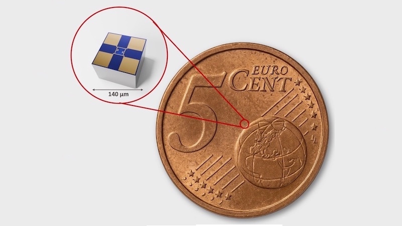
This shows the scale of how ultra tiny Digid’s nanoscale sensors are.
Digid reports that the process now supports automated wafer-level manufacturing with production plans scaling from early low-volume runs to millions of sensors per year.
All About Circuits talked with Dr Konstantin Kloppstech, Chief Technology Officer of Digid, and Dr. Nils Könne, Head of Product at Digid, to learn more about the milestone firsthand.
Architecture of a Printed Nanoscale Sensor
Whereas conventional miniaturized sensors are based on MEMS micromachining, Digid’s sensors rely on a printed piezoresistive architecture. The company deposits conductive and resistive structures directly onto a target substrate using an automated process that resembles additive manufacturing at the micrometer scale.
Each sensor forms a complete resistive sensing element. In force-sensing configurations, Digid can even implement full Wheatstone bridge topologies within footprints on the order of a few square micrometers.
The company fabricates sensors at wafer scale, starting from 4-inch wafers that host roughly 12,000 individual systems prior to deposition. As Dr. Kloppstech explains, “We start on a four-inch wafer with about twelve thousand individual systems, and we print the sensors to each one in an automated process.”
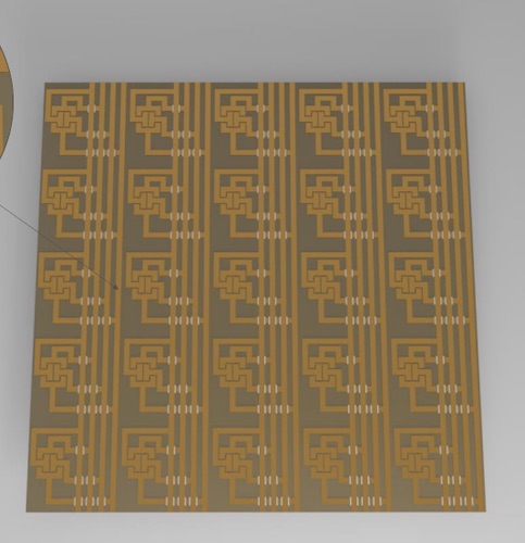
A printed force-sensitive polymer array
The printed structures define the sensing geometry, while the underlying material serves as the mechanical or thermal interface. With this approach, Digid eliminates the need to carve cavities, membranes, or suspended structures into the host material, making for notably simpler integration and improved mechanical integrity.
Importantly, the electrical readouts use standard voltage or resistance measurements, meaning engineers can directly interface the sensors with conventional ADCs. Digid also reports that it can tune baseline resistance values to accommodate low-cost or low-precision electronics for simpler systems and less power overhead.
Integrated Functions at Nanometer Scale
Despite their size, Digid’s sensors integrate multiple functional layers. At the most basic level, each printed structure incorporates the sensing element, interconnects, and contact pads. Force sensors exploit piezoresistive effects, while temperature sensors rely on precisely characterized resistance changes with temperature. Digid emphasizes that the sensors exhibit highly linear responses and negligible self-heating due to their extremely low thermal mass.
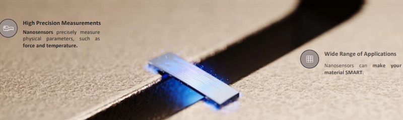
Digid’s vision includes printing nanosensors directly onto parts.
While designers still need to externally implement signal conditioning, Digid supplies supporting firmware and software that convert raw resistance or voltage changes into calibrated temperature or force values. As Kloppstech explains, “We offer our sensor technology as an end-to-end solution.”
“If our engineer customers are interested in readout and signal processing, we have software in-house for analyzing data and calibrating signals.”
By separating the physical sensing element from signal processing and control logic, Digid allows the physical sensor to remain minimal while offering closed-loop control at the system level. The company claims the sensors require no drift compensation or nonlinear correction, which is a differentiator from many MEMS-based alternatives.
Toward 10 nm and Beyond
Digid’s current production sensors measure roughly 1 µm in length, with force-sensing arrays achieving individual element sizes of approximately 5 x 5 µm2 {SUPERSCRIPT}, while their polymer-based force sensors can reach thicknesses near 10 µm while integrating full Wheatstone bridges.
To date, Digid has produced more than 1 million sensors in its in-house cleanroom and plans capacity expansions toward multi-million-unit annual output using fully automated deposition lines.
The company also has a roadmap to 10 nm-scale devices, which would be a two orders-of-magnitude reduction in linear dimensions relative to current offerings. As Kloppstech describes, “What you see here is roughly a micrometer in length today, but from a technology point of view, we are not limited there. We can push this down toward transistor dimensions.” At transistor-class feature sizes, which fundamentally changes where and how sensing can occur.
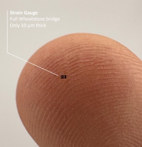
Digid’s 10um-thick Wheatstone bridge strain gauge
For example, designers could use such tiny sensors to distribute sensing elements at densities comparable to biological systems. Tactile or thermal arrays could then approach the granularity of human nerve endings. In robotics, for example, such density could unlock surface-level force and temperature mapping on end effectors without altering form factors.
In electronics, nanometer-scale thermal sensors could unlock direct placement within thermal interface materials, on bare silicon dies, or inside future 3D packaging stacks. The corollary would be real-time thermal load balancing, localized throttling decisions, and improved reliability through early hotspot detection. Digid estimates that such thermal insight can substantially reduce failure rates and cooling costs in high-performance systems.
You can learn more about Digid’s nanosensors at the company’s Nanosensor Technology page.
A Pervasive Sensing Layer
One of Digid’s early deployment targets is the medical device industry, as the company already holds ISO 13485:2016 certification. To Digid, the future looks bright, says Kloppstech.
“Now we are at a point where sensing can go exactly where it was never possible before, without changing the original function of the material or device.”
QUOTE
All images used courtesy of Digid.