Facebook
 Google
 GitHub
 Linkedin
Keysight’s Machine Learning Toolkit to Speed Device Modeling and PDK Dev
The new toolkit integrates with Keysight’s device modeling software to automate parameter extraction and shorten compact-model and PDK development cycles.
Keysight Technologies has introduced a machine learning toolkit to accelerate device modeling and process design kit development, addressing a long-standing bottleneck in advanced semiconductor design flows. Delivered as part of Keysight’s Device Modeling Software Suite, the toolkit automates compact-model extraction, reduces manual tuning, and supports faster design-technology co-optimization.
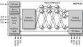
Keysight's Model Builder Pro 2026 has a new Machine Learning Toolkit (MLT) and Python automation framework.
The Machine Learning Toolkit (MLT) targets teams responsible for building and maintaining device models in circuit simulation and PDK delivery. Compact-model development has become an increasingly important path item that can take weeks or more as device architectures become more complex. Keysight designed MLT to compress that timeline by embedding machine learning-driven optimization and automation directly into established modeling workflows.
Augmenting Existing Workflows
The MLT is integrated into Keysight’s Model Builder Pro platform, with support spanning recent releases of Model Builder Pro and IC-CAP. Rather than introducing a standalone modeling environment, Keysight has implemented the toolkit as a set of workflow components that augment existing extraction and validation workflows.
According to Keysight, the MLT’s primary benefit is reduced manual parameter extraction work. Traditional compact-model development usually involves hundreds of iterative adjustments to fit measured device data across bias conditions, geometries, and temperatures. The new toolkit uses an ML-based optimizer to perform global parameter extraction, allowing dozens of parameters to be optimized simultaneously in a single run, reducing 200-step extraction flows down to fewer than 10 automated ones.
Keysight also emphasizes Python-based customization in the MLT, enabling modeling teams to script extraction flows, automate corner adjustments, and build utilities around the ML optimizer. This approach is intended to make modeling workflows more repeatable and easier to adapt as device targets evolve.
A Scaling Problem
Compact models have grown steadily more complex as new device structures introduce additional second-order effects that must be captured accurately for circuit simulation. Keysight points to advanced logic architectures such as GAA transistors, as well as wide-bandgap devices including GaN and SiC, as examples where parameter counts and interdependencies have increased.

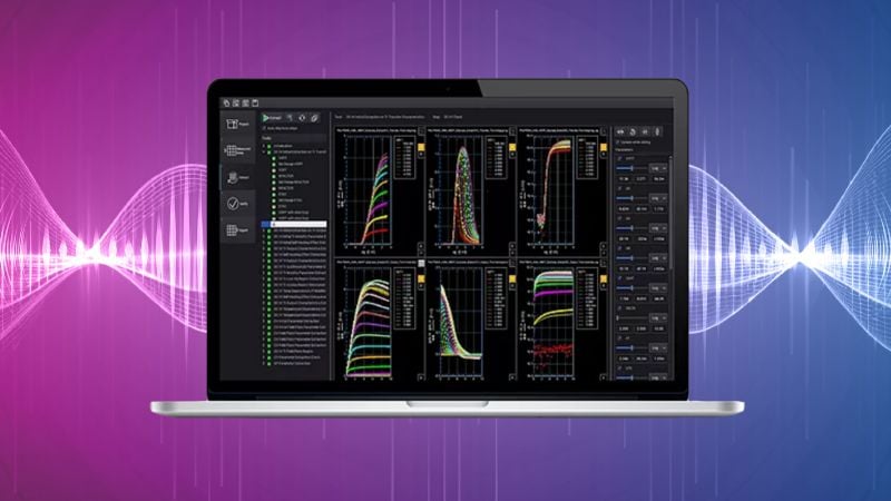
Example of the benefits of modeling with the Keysight ML Optimizer.
At the same time, PDK schedules are also under pressure. A PDK packages device models, verification rules, and technology files into a form that designers can use inside EDA tools, and delays in model availability can stall circuit development and hamper progress. As foundries and integrated device manufacturers push tighter integration between process development and circuit design, compact-model extraction has become a gating factor for effective design-technology co-optimization.
Ultimately, Keysight’s messaging with the MLT centers on turning what has traditionally been a manual, expert-driven process into a more automated pipeline step. The ML optimizer is described as derivative-free and capable of learning from evaluation results during extraction, which is intended to reduce sensitivity to initial conditions and local minima that can complicate conventional optimization methods.
From Weeks to Hours
In terms of workflows, MLT’s most immediate impact for designers is turnaround time. Keysight claims that model development tasks that previously took weeks can be reduced to hours, and that PDK update cycles can be shortened from weeks to days when integrated into DTCO loops.
The toolkit also aims to improve consistency. Manual extraction depends heavily on individual expertise, making results difficult to reproduce across teams or projects. But by encoding extraction flows and optimization strategies into automated scripts, the toolkit can standardize modeling practices while still allowing expert oversight.
Keysight does, however, acknowledge that optimization effectiveness can decline as parameter counts climb into the hundreds, and that compute requirements scale with model complexity and data volume. The toolkit is not presented as a one-click solution for every modeling challenge, but rather as a way to reduce repetitive manual work and free specialists to focus on model structure and validation rather than on parameter tuning.
Keysight’s MLT reflects a broader trend in EDA and semiconductor development toward embedding machine learning into established tools rather than building separate AI-centric workflows. By integrating ML-driven extraction into its existing device modeling platforms, Keysight is targeting adoption by teams that already rely on those tools for PDK delivery and device characterization.