Facebook
 Google
 GitHub
 Linkedin
Researchers Rethink the Transistor at a Material Level
While many researchers focus on the miniaturization of the transistor, others are looking to materials science to advance this building block of modern electronics.
Transistors are reaching their physical limits in size and speed. As transistors are made smaller, the distance between the source and drain decreases, leading to high leakage currents. And as the transistor size approaches the atomic level, it is difficult to control the current flow, leading to a higher probability of computation errors.
Smaller transistors mean slower switching speeds, which is especially problematic in newer applications like artificial Intelligence, where massive datasets need to be processed. Denser integration also becomes a challenge because of stacking and thermal management issues.
This article discusses recent research developments that push the boundaries of existing transistor technologies and how they may outperform current devices.

Below, we'll discuss a wood-based transistor developed by researchers at Linköping University and the KTH Royal Institute of Technology, among other transistor research breakthroughs. Image courtesy of Thor Balkhed/Linköping University
Growing 2D Materials on a Silicon CMOS Wafer
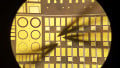
Current transistors are bulky and cannot be easily stacked vertically for high density. For such integration, transistors must be made of ultrathin 2D materials, which are only a few atoms thick. However, growing 2D materials on a silicon wafer is challenging because it usually requires a temperature of around 600°C—and circuits can only withstand up to 400°C.
To tackle these issues, Massachusetts Institute of Technology (MIT) researchers have developed a low-temperature process to grow 2D materials on-chip without damaging them. The new process reduces the time it takes to create the 2D materials and creates a uniform layer over the entire surface area. As a result, the new process can be used for larger surfaces than conventional processes.

Graduate student Jiadi Zhu holding the wafer developed with the new process. Image courtesy of MIT
The MIT researchers focused on molybdenum disulfide, a transparent and flexible material with electronic and photonic properties, for demonstrating and validating their new process. Their process is placed in an oven with two chambers: a low-temperature region in the front and a high-temperature region in the back. The wafer is placed in front so it remains intact. Vaporized molybdenum and sulfur precursors are pumped into the furnace. Molybdenum stays in the front, and sulfur precursor flows in the high-temperature region to decompose. After decomposition, it flows back to the low-temperature chamber, where the molybdenum disulfide grows.
The researchers placed the wafer vertically in the front chamber so neither edge was too close to the high-temperature region. They also deposited a thin layer of passivation material on top of the chip to prevent the sulfurization of metals like aluminum and copper, commonly used in silicon circuits for connecting a package or carrier. The passivation layer is later removed to make connections. The researchers plan to fine-tune their technique and explore the application of this process for flexible surfaces like polymers, textiles, and papers.
New Material Contends With Silicon-based Transistors
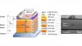
Researchers at Forschungszentrum Jülich have explored materials with more favorable electronic properties than silicon for better-performing circuits. They recently fabricated a germanium-tin alloy that has many benefits over conventional silicon transistors.
Germanium exhibits higher electron mobility than silicon. The researchers added tin atoms into the germanium lattice to further optimize the material's electronic properties. The new alloy's electron mobility is 2.5 times higher than pure germanium transistors and is compatible with the current CMOS fabrication process.

The germanium-tin transistor design. Image courtesy of Forschungszentrum Jülich
The new transistors work at temperatures down to 12 Kelvin—an important improvement to existing transistors that need high voltage to switch at temperatures below 50 Kelvin, consuming more power. The scientists claim that with further improvements, their alloy may even allow transistors to operate at temperatures lower than 12 Kelvin. The team believes their technology is a promising candidate for next-generation, low-power, high-performance chips and possibly for the future of quantum computers.
Transistors Made of Wood
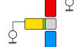
Researchers at Linköping University and the KTH Royal Institute of Technology have created a transistor with wood. They used balsa wood, a grainless, evenly-structured wood, for this application. They removed lignin, leaving only cellulose fibers with channels, which were then filled with a conductive polymer called PEDOT:PSS.
The team found that their device regulated electric current and provided continuous operation at a selected output level. However, the switching time was very long. It took about a second to turn off and five seconds to turn on.

Components of the wood transistor. Image courtesy of Linköping University
According to the researchers, these organic transistors can be used for high-power applications since they can withstand high currents. While the team has not created this device for any specific application, they hope their research will pave the road for future organic electronics.
Related Content