Facebook
 Google
 GitHub
 Linkedin
Lattice Leverages FD-SOI for New Low Power FPGAs
AAC sat down with Lattice Semiconductor to hear about its newest FPGA offering, which claims lower power compared to competitors. However, how does it back up this claim?
In many of the world’s electronic applications today, low power is the name of the game. However, high levels of integration and device scaling have created a power/performance/reliability tradeoff that has mostly halted traditional power scaling methods.
One technology used in the industry to mitigate this tradeoff is fully depleted silicon-on-insulator (FD-SOI) technology which can operate at 75% lower power as compared to a bulk CMOS process. Lattice Semiconductor continues to reap the benefits of FD-SOI with its newest FPGA offerings. These offerings claim to be some of the company’s lowest power yet, and they cite FD-SOI as a key source.

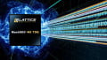
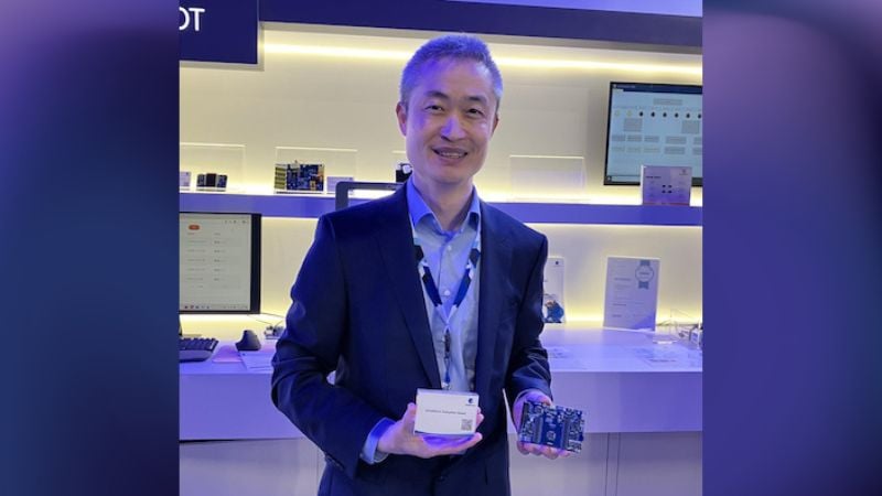
Lattice's newest FPGA, the CertusPro-NX. Image used courtesy of Lattice Semiconductor
This week, All About Circuits had the chance to sit down with JuJu Joyce, Product Marketing Manager from Lattice, to hear about the new offerings and how they stack up to the competition, first hand.
A History of Scaling and Power Consumption
Historically, decreasing power consumption in a digital IC was reasonably straightforward. Directly from the classic dynamic power equation, it was clear to see that dynamic power consumption would decrease with the square of the supply voltage.
\[P_{dynamic} \Rightarrow {fC_LV_{DD}}^2\]
However, lowering the supply voltage, Vdd, will, in turn, reduce the gate-to-source voltage (Vgs) available to drive the transistors. As the MOS saturation current equation shows, this reduced gate voltage reduces the drain current. Since lower currents mean slower charging/discharging of capacitive nodes, it becomes clear that lowering Vdd will also have the unintended effect of decreasing speed and performance.
\[I_{D,sat} = \frac{\mu _p \cdot C_{ox}}{2} \cdot \frac{W}{L} \cdot (V_{GS} - V_T)^2\]
To address this, the CMOS industry again turned to the MOS saturation square law equation. Using this equation, designers noticed that if they could decrease the threshold voltage (Vt) as much as they reduce Vgs, the loss in speed could be offset while keeping the decrease in dynamic power consumption, thus a potential win-win situation.
Though this method may seem like an easy enough solution, more challenges started to arise, bringing the need for a new possible solution.
FD-SOI
For a while, this mathematical technique worked; however, as threshold voltages decreased, so did the sub-threshold region. Eventually, this led to increased leakage currents. Essentially, the transistors do not turn off very well. At the same time, mass integration resulted in billions of transistors on a single chip.
Suddenly the sum of individual threshold leakages was far from trivial, and designers could no longer afford to lower supply voltage and threshold voltages.
To address this need, many semiconductor companies have turned to FD-SOI technology. FD-SOI technology is very similar to conventional bulk CMOS but crucially adds two features: an extremely thin transistor channel and an insulating buried oxide underneath the channel. This extremely thin transistor channel can be beneficial since it doesn’t need to be doped (hence fully depleted).
![]()
FD-SOI allows for better channel control and decreased leakages. Image used courtesy of STMicroelectronics
This innovation resulted in a drastic improvement in transistor subthreshold behavior, significantly decreasing transistor subthreshold leakages and improved control of electrons in the channel. With reduced leakage currents, designers could continue decreasing supply voltage to lower dynamic power consumption. Controlling the back-bias voltage below the buried oxide layer can also be used to dynamically adjust the threshold voltage; lower for increased speed and higher for reduced leakage current.
Lattice’s New Offerings
Today, Lattice Semiconductor announced its new family of Nexus FPGAs with its CertusPro-NX offering.
Designed specifically for low power and high interface bandwidth, the new FPGA offers up to 100K logic cells, embedded memory, DSP blocks, and 8 SERDES lanes that can achieve up to 10 Gbps in bandwidth, which claims can be up to 2x more than the closest competition. Also, coming in a 9x9 mm form factor, the FPGA has up to 7.3 Mb of on-chip memory, including LPDDR4 and DDR3 at 1066 Mbps.

Block diagram of the Lattice CertusPro-NX. Image used courtesy of Lattice
One of the most exciting aspects of the new FPGA from Lattice is the low power consumption it offers.
As Joyce explained to us: “We are using a low power design that is built on FD-SOI technology that comes with its own inherent power advantage... And then sitting on top of that is our Lattice architecture that is optimized for power efficiency.”
This device operates at a supply voltage of 1V and is built in a 28nm FD-SOI process. The result, according to Lattice, is up to 4x lower power consumption at 5 Gbps and 10 Gbps than its closest competitors (e.g., Xilinx Artix-7).

CertusPro-NX power consumption vs its close competitors. Image used courtesy of Lattice Semiconductor
Part of this power-saving architecture is the high amounts of integrated on-chip memory that the CertusPro-NX is offering.
Thinking specifically about edge computing, Lattice wanted to limit off-chip memory accesses to lower power consumption and improve performance.
Joyce explains, "we have recognized this need and have put in ample amounts of internal memory. Now, users don't have to go out to an external memory like the RAM to fetch data as frequently.. and that means now they can run their processing much faster."
Moving Forward
Moving forward, Lattice plans to extend support of their Lattice Sensai, Lattice mVision, and Lattice Automate stacks to the CertusPro-NX. The hope is that its new FPGA can support a plethora of edge AI applications while also benefiting users with the device's decreased area and power consumption.
When it comes to this new device, Lattice is "excited about all the new possibilities that this device will open up for [its] customers and the new capabilities that they will get from a system design standpoint."
Interesting in past Lattice Semiconductor news? Find out more in the articles down below.
Lattice Semiconductor Guards Against Firmware and Supply Chain Attacks
FPGA Roundup: New Contenders Hone in on Memory, Size, Power, and Even AI
FPGAs and Firmware: An Ironclad Security Duo at Every Stage of Design and Manufacture