Facebook
 Google
 GitHub
 Linkedin
A New 45V Zero-Drift Op-Amp from Microchip, the MCP6V51
This article looks at Microchip’s MCP6V51, which is a zero-drift operational amplifier with a wide supply range and enhanced EMI rejection.
This article looks at Microchip’s MCP6V51, which is a zero-drift operational amplifier with a wide supply range and enhanced EMI rejection.
The MCP6V51 has a maximum offset voltage of 15 μV, exhibits an offset voltage drift of 36 nV/°C, and offers an integrated input noise voltage of 0.21 μVp-p from 0.1 Hz to 10 Hz. The device supports a wide supply range from 4.5 V to 45 V and has a quiescent current of 470 μA. A single or dual supply can be employed to operate the MCP6V51.

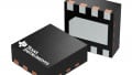
The MCP6V51 is offered in an 8-pin MSOP package (left) and a 5-pin SOT-23 package (right). Image from Microchip
The minimum power supply rejection ratio (PSSR) and common-mode rejection ratio (CMRR) of the device are 134 dB and 135 dB, respectively. Industrial instrumentation, sensor conditioning, and power control loops are some of the important applications of this op-amp.
Let’s take a closer look at some of the salient features of the MCP6V51.
Zero-Drift Operation
Let's start by taking a look at the functional diagram of the MCP6V51, shown below.

Functional diagram of the MCP6V51. Image from Microchip.
The main amplifier has two sets of differential inputs. The upper differential inputs are directly connected to the inputs of the MCP6V51 (VIN+ and VIN-). This path is designed for high gain and high bandwidth. The lower differential inputs are connected to the output of an auxiliary path which is formed by the chopper input switches, auxiliary amplifier (aux. amp.), chopper output switches, and the low-pass filter. This path has a lower bandwidth (because of the low-pass filter and the switching functionality employed in the choppers).
The auxiliary path has some switching networks within the chopper circuits. The arrangement of these switches is changed periodically and the op-amp offset voltage is effectively reduced. Refer to my article on the OPA2333P op-amp from Texas Instruments to read about the details of offset cancelation techniques in a basic zero-drift amplifier.
The signals from the two differential pairs of the main amp are internally added together and passed on to Vout through the output buffer.
The oscillator produces the clock signal to drive the switching network of the chopper circuits.
The power-on reset (represented in the POR) ensures that the device starts in a known state when power is first applied to the device.
Input Common Mode Range
The input common-mode voltage of the MCP6V51 can go 0.3 V below the negative rail. This can be helpful for low-side current sense applications as shown below.

Image courtesy of Microchip.
We should ensure that the voltage present at the non-inverting input of the MCP6V51 is within the common-mode range of the device. This voltage can be negative if the load current is bidirectional. In this case, we have to choose Rshunt in a way that the absolute value of IL ✕ Rshunt is less than 0.3 V. Hence, designing with different op-amps, we should consider the common-mode range that the device supports. For example, with the OPA2333P from Texas Instruments, the common-mode range extends 0.1 V beyond the supply rails.
The maximum input common-mode for the MCP6V51 is VDD-2.1 V. Hence, the device more easily lends itself to low-side current sensing than to high-side current sensing where the common-mode voltage is close to the supply.
Output Voltage Range
The MCP6V51 has a rail-to-rail output ranging from VSS+50 mV to VDD-100 mV. This is fine for many applications but if your particular application requires swinging very close or even slightly below the negative rail, then you should consider an op-amp such as the OPA2333P.
Integrated EMI Filter
The MCP6V51 incorporates integrated 2nd-order RC low-pass filters to suppress electromagnetic or RF interference. These filters, which have a bandwidth of 115 MHz, lead to the EMI rejection shown in the graph below.

Image courtesy of Microchip.
As you can see, a 900 MHz interfering signal experiences an attenuation of about 95 dB.
Thermal Shutdown
The MCP6V51 has internal thermal shutdown circuitry that becomes activated when its die temperature goes above approximately 175°C. The ambient temperature and/or the amplifier’s output current can trigger the thermal shutdown circuitry. Hence, the designer should take these parameters into account.
When in thermal shutdown mode, the op-amp output becomes high-impedance. The output won’t be enabled again unless the temperature reduces to approximately 160°C.
You can find more information on this subject in the device datasheet.
Low-Frequency Noise Performance
The MCP6V51 is a zero-drift device and has “virtually no” flicker noise. The integrated input noise from 0.1 Hz to 10 Hz is 0.21 μVp-p.

Image courtesy of Microchip.
CMRR, PSRR, and Open-Loop Gain
The "minimum" PSRR and CMRR of the MCP6V51 are 134 dB and 135 dB, respectively. Additionally, the device has open-loop gain of 140 dB. For the OPA2333P, we have PSRR, CMRR, and open-loop gain of 120 dB, 106 dB, and 106 dB, respectively. These comparisons may not be 100% fair because the test conditions are not the same, and also the “typical” CMRR and open-loop gain for the OPA2333P are both 130 dB. However, judging only with these numbers, it seems that the MCP6V51 exhibits better performance considering the DC specifications.
Note that a lower PSRR increases offset error. Let’s consider a circuit in which a battery is used to power the amplifier. During the life of the battery, the supply changes by 1 V. Suppose that the reciprocal of the power supply rejection ratio of the whole amplifying stage is 500 μV/V. The input offset error will increase by 1 V ✕ 500 μV/V, which gives 500 μV by the end of the life of the battery. If the reciprocal of the PSRR were only 1 μV/V, the offset variation would be only 1 V ✕ 1 μV/V= 1 μV.
In this article, we looked at some of the most important features of the MCP6V51. The device supports a wide supply ranging from 4.5 V to 45 V. It has integrated EMI filters to suppress high-frequency interference and employs a thermal shutdown mechanism. In addition, the DC specifications of the device, such as PSRR, CMRR, and open-loop gain, are noteworthy.
Related Content