 Facebook
 Google
 GitHub
 Linkedin
A nanoPower and Tiny Voltage Supervisor from Maxim (and They Aren’t Kidding about the “Tiny”)
A look at the MAX16140—a tiny device that uses a tiny amount of current, but one that promises a lot.
In this article, we take a look at the MAX16140, a tiny device that uses a tiny amount of current, but one that promises a lot.
The chosen term “tiny” is an understatement when describing the physical size of the MAX16140. At 0.78mm × 0.78mm × 0.5mm, this IC is unbelievably small. If you’re looking for a voltage supervisor to be hand-placed, just keep on looking because—unless you’re a brain surgeon or your name is Data, from Star Trek—you most likely won’t possess the steady hand or the patience needed for placing this teeny-tiny IC, meaning you’ll definitely need pick-and-place automation equipment.

The MAX16140 (not to scale). Image from Mouser.
The advertised tiny—or nanoPower, as Maxim refers to it—amount of quiescent current required to operate this device is a mere 370nA. Keep in mind, however, that this typical spec is valid only at 25°C. But still, the quiescent current levels at elevated temperatures and voltages are impressive nonetheless (see image below).

Figure 1. Supply Current vs. Supply Voltage. Image taken from the datasheet.
Factory-Programmed ICs
Although this voltage supervisor has a relatively wide operating voltage range, from 1.7V to 5.5V, this IC can’t monitor supply voltages up to 5.5V. Rather, it’s promoted as being able to monitor voltages ranging from 1.7V to 4.85V with very small, impressively small, increments of 50mV. The downside is that this device is not made for end-user customization; you must order the pre-programmed (i.e., factory-programmed) IC with your desired settings. And if you’re hoping to pinpoint the exact voltage threshold for your design through trial and error, then you would need to order a variety of different, pre-programmed, voltage threshold settings. Fortunately, Maxim has made this selection process easy via their Selector Guide (see image below).

Figure 2. The selector guide. Image taken from the datasheet.
Be Careful with Copy and Paste
Maxim has been generous with providing detailed information about this device, including reset, voltage threshold, and time-delay specs, as well as explanations of the IC’s pins (technically called “bumps”), and application information such as power supply bypassing and grounding (page 9 of the datasheet).
However, they made a goof with their supply current vs. supply voltage graph. Apparently, this device can operate from a supply voltage of -40V to an astounding 125V! See figure below. They forgot to re-label the graph’s title to Supply Current vs. Temperature, and then also to change the graph’s x-axis label. [Update: Maxim reached out to let us know that they've corrected the graph on page 4 and updated the datasheet since the time of publication.]
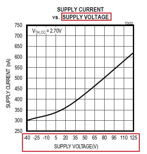
Figure 3. A documentation goof (-40 to 125 supply voltage range). Image taken from the datasheet. [Note: Maxim has updated the datasheet with a corrected plot.]
Manual Reset—A Useful Feature
It’s nice to see that Maxim realizes that these ICs, when added to a design, will eventually require manual testing. The manual reset input (MR) feature was added specifically for this purpose.
According to the datasheet, the factory-programmable manual reset input capability allows “the operator, a test technician, or external logic circuit to initiate a reset” via a rising-edge, a falling-edge, an active-low, or an active-high input signal. From my own experience as a test and validation engineer, I can tell you that these MR options will be very valuable when ringing out bugs or when approaching other troubleshooting, or management-driven feature creep…smiley face, issues. Refer to Figure 2 above for the factory-programmable MR input configuration options.
Wafer-Level Package Information
If you've never used a WLP (wafer-level package)—this is the magic that allows these devices to be so tiny—then you’ll want to get educated on how to properly design your PCB for accommodating them, to make sure your board house has the capabilities for making appropriate landing pads, and (this is critically important) to ensure your assembly house (i.e., the pick-and-place machines) can confidently handle and place these devices. Fortunately, Maxim has provided, within the datasheet, a WLP land pattern application note. Unfortunately, the datasheet link DOESN’T WORK! Luckily, I was able to quickly locate the app note thanks to Mr. Google. [Update: The URL is working now.]
One final note: I’ll share a lesson with you that I gained through experience when using WLPs. It’s always a good idea, actually a great idea, to closely surround a WLP device with other devices (resistors, caps, other more robust ICs, etc.). The goal here is simply protection—WLPs can easily (and literally) be knocked off a PCB merely by handling, even carefully handling, the PCB. And if you don’t have any spare or otherwise convenient devices to protect the WLP with, then add some inexpensive surface-mount resistors or caps, and just leave their terminals unconnected.
Have you had a chance to use these new voltage supervisors? If so, leave a comment and tell us about your experiences.


Hi guys,
I have drawn a few reference voltage supervisor schematics with various IC. You can check out these links, and use these with ESP32 for voltage supervision. Let me know any questions you have in your mind.
https://www.flux.ai/ramprakashvishnoi8/tps3839-with-a-boost-converter-tps6126x
https://www.flux.ai/ramprakashvishnoi8/tps383xxras-piesp32stm32
https://www.flux.ai/ramprakashvishnoi8/ka75330