 Facebook
 Google
 GitHub
 Linkedin
Nexperia’s Latest MOSFET Targets Load-switch and Hot-swap Applications
This article examines the PSMNR51-25YLH and discusses MOSFET drain-source leakage current.
An idealized MOSFET is a marvelous device.
We apply an appropriate voltage to a perfectly insulated gate and current flows freely from drain to source. Once we start to learn about all the little details of MOSFET operation, we might almost feel a bit of nostalgia for this vastly oversimplified model.
Drain-to-source resistance, gate resistance, parasitic capacitances, the body effect, avalanche breakdown…. There seems to be no end to the imperfections that complicate the design and implementation of MOSFETs, and in this article, we’ll explore a nonideality known as drain-source leakage current and abbreviated IDSS.
MOSFET Drain-to-Source Leakage
We expect a MOSFET to prevent current flow from drain to source when we apply a gate-source voltage that is far below the threshold voltage, and this is indeed what the device does—well, more or less. Some current will flow even when the MOSFET is in the off state, and manufacturers convey information about this “leaking” current by reporting values for IDSS.
In an application note on power MOSFET parameters, Taiwan Semiconductor defines IDSS as the current that flows from drain to source when the gate is shorted to the source and the device’s maximum drain-source voltage is applied.
This definition seems to be fairly standard, though the datasheet for Nexperia's new PSMNR51-25YLH reports IDSS at a drain-source voltage of 20 V, rather than at the maximum, which is 25 V.

Diagram of IDSS. Image used courtesy of Taiwan Semiconductor
Drain-source leakage increases significantly as temperature increases. Nexperia indicates that the PSMNR51-25YLH exhibits good IDSS performance even at high temperatures.
Should We Be Worried?
Drain-source leakage is undesirable simply because it leads to wasted power. The leakage current multiplied by the drain-source voltage represents power dissipation that is occurring whenever the transistor is inactive.
However, drain-source leakage currents tend to be very small, and this makes me wonder why Nexperia emphasizes low IDSS in its description of the PSMNR51-25YLH. Reduced channel length contributes to drain-source leakage, and consequently, IDSS is a nontrivial concern with newer integrated circuits, since the numerous short-channel transistors in a VLSI chip will create significant amounts of static power dissipation.
The PSMNR51-25YLH, though, is a discrete FET intended for power applications. Thus, I can only assume that the importance of IDSS in this context reflects the desire to maximize energy efficiency even in systems that are not constrained by the need to extend battery life or reduce heat generation.
Logic-Level Power Control and Load Switching
The PSMNR51-25YLH supports fairly high drain-source voltages and extremely high drain currents (380 A), and yet its gate-source threshold voltage is only 1.55 V (typical) and its on-state resistance starts to flatten out at around 5 V.

RDS(on) as a function of gate-source voltage. Image used courtesy of Nexperia
Thus, you can control the FET using a typical 3.3 V logic signal from a microcontroller, and if you want to reduce RDS(on) almost to the minimum, all you need to do is translate that 3.3 V signal to 5 V.
And while we’re on the topic of on-state resistance, I really was surprised when I saw the RDS(on) spec for this FET: 0.82 mΩ maximum at VGS = 4.5 V. Less than one milliohm is some seriously low resistance!
Thermal Design
One thing that I like about the PSMNR51-25YLH is related not to the part itself but to the datasheet. Thermal issues are a critical and easily overlooked aspect of power design, and most electrical engineers don’t have the expertise or the resources needed to perform advanced thermal analysis. Thus, the assistance offered by the manufacturer is greatly appreciated.
In the case of the PSMNR51-25YLH, the datasheet includes two examples of PCB layouts and provides specs for junction-to-ambient thermal resistance that corresponds to these examples.

Diagrams and specifications relating to PSMNR51-25YLH's thermal resistance. Image used courtesy of Nexperia
This is valuable information that helps the designer to estimate the amount of copper area required to maintain acceptable temperatures in a given application. (For more information on this topic, refer to my article on thermal design for linear regulators.)
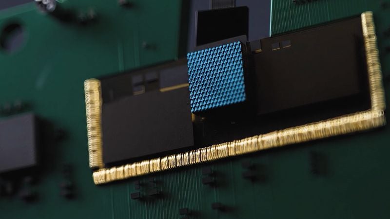
Feature image (modified) used courtesy of Nexperia
I’m still curious about why IDSS might be considered a prominent spec in the context of a transistor such as the PSMNR51-25YLH. If you have any thoughts, feel free to share them in the comments.


driving a high impedance load like a micro or an LED will cause the LED to glow with >10uA leakage.
An ‘ideal’ or ‘perfect’ mosfet achieves zero leakage in the OFF state, and achieves zero resistive losses in the ON state. Impossible to achieve, but PSMNR51-25YLH comes closer than many competitors
Choosing a mosfet with low IDSS leakage can extend the battery life of a notebook computer, mobile phone or even a family car
Switching regulators use Schottky diodes to reduce voltage spikes and body-diode losses, but Schottky technology suffers from high IDSS(hot) leakage. A 25V mosfet can have several mA of leakage at >100C which can have a massive effect on battery life or efficiency.
Nexperia’s unique low-voltage superjunction technology has a different type of body diode, “SchottkyPlus” technology delivers Schottky-like performance and around 1000x lower hot IDSS leakage than mosfets with integrated Schottky diodes.
Finally, IDSS leakage occurs because of tiny imperfections in the silicon die. As these defects get bigger or more prolific, then leakage increases accordingly., a perfect mosfet has zero leakage.
Low IDSS leakage is a good indicator of low defectivity. If devices with high leakage are removed during production test, then this is a great way to ensure that the remaining devices shipped to customers meet the toughest quality & reliability requirements of the automotive & telecom industries such as AECQ101