Facebook
 Google
 GitHub
 Linkedin
NVIDIA Boasts “World’s Most Advanced Chip” in Latest Tensor Core GPU
Taking aim at creating a future supercomputer, NVIDIA has created a new H100 Tensor Core graphics processing unit (GPU) leveraging its latest architecture, Hopper.
Thanks to its GTC conference, NVIDIA has pumped out a plethora of newer technology, like the Grace central processing unit (CPU) "Superchip" and Hopper architecture.
Still, amongst all of the releases, one that may stand out the most is the company's newest GPU, the H100.

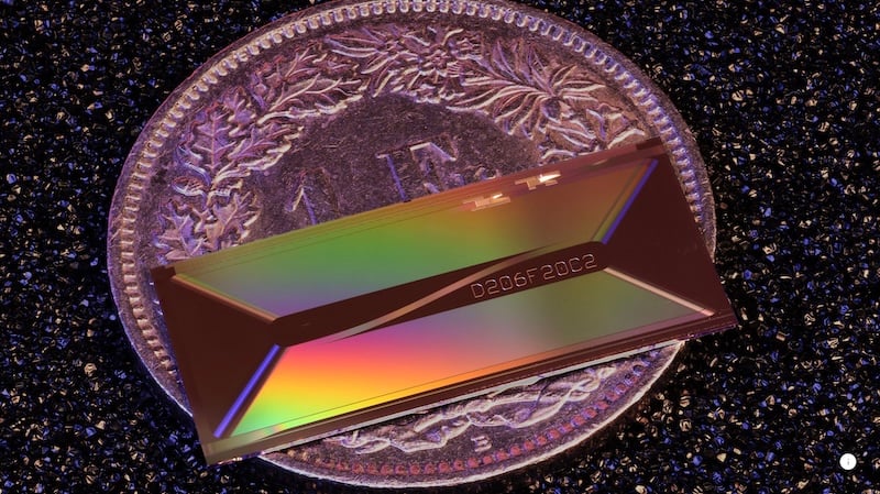
The H100 Tensor Core GPU. Image used courtesy of NVIDIA
In this article, we'll look at the new H100 Tensor Core GPU from NVIDIA to see how it works, what it offers, and how it could impact the industry.
NVIDIA's Tensor Core H100 GPU
Arguably the crowning achievement for NVIDIA at this year's GTC Conference was the release of its new H100 Tensor Core GPU.
The H100 is NVIDIA's first GPU built off of its new Hopper architecture, and, as such, NVIDIA is calling it the "World's Most Advanced Chip."
Built off a cutting-edge TSMC 4N process, the new GPU integrates 80 billion transistors into a single die. Designed for scale-up and scale-out infrastructures, the new GPU prioritizes bandwidth and data rates for networking, chip-to-chip communication, and I/O.
To this end, the new GPU claims to support 40 TB/s of I/O bandwidth and 3 TB/s of memory bandwidth, largely due to H100 being the first GPU to support PCIe Gen5 as HBM3.
CEO Jensen Huang explains, "Twenty H100 can sustain the equivalent of the entire world's internet traffic."
Thanks to a series of new Hopper architecture improvements, the H100 is also a workhorse for AI applications. Specifically, the GPU is capable of 4 PFLOPs of FP8 and 2 PFLOPs of FP16, marking a 6x and 3x improvement over Ampere GPUs, respectively.
NVIDIA said that when training models such as Mixture of Experts, H100 enabled 9x faster training than previous technologies.
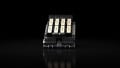
DGX H100 Systems
To deploy the H100 GPU, NVIDIA also announced its fourth-generation DGX system, dubbed DGX H100.
DGX H100 systems are equipped with eight H100 GPUs, each connected with NVIDIA NVLink interconnect technology.
In this configuration, DGX H100 can achieve 32 petaflops at FP8, scaled up even further with the DGX POD and DGX SuperPOD systems. These can then connect a series of DGX H100 nodes through NVIDIA's new NVLink Switch System.
The DGX SuperPOD can connect up to 32 nodes, equaling 256 H100 GPUs, to achieve one exaflop of FP* AU Performance.

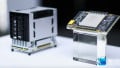
Rendering of a fourth-generation DGX system. Image used courtesy of NVIDIA
To top it all off, NVIDIA plans to use its DGX SuperPODs to build the world's fastest AI Supercomputer.

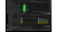
A high-level comparison of SuperPODs between the DGX A100 and DGX H100. Screenshot used courtesy of NVIDIA [downloadable whitepaper]
Dubbed the NVIDIA Eos, the supercomputer will combine 576 DGX H100 systems, totaling 4,608 H100 GPUs.
Altogether, NVIDIA anticipates this supercomputer reaching 18.4 exaflops of aI compute, a number which is 4x faster than the next closest AI supercomputer.
H100 Deployment
NVIDIA is undoubtedly raising the bar this year by shattering its previous best performances and even setting some world records along the way. Yet, more impressive than the technology itself is the response that it's getting from the industry.
According to NVIDIA, companies including Atos, BOXX Technologies, Cisco, Dell Technologies, Fujitsu, GIGABYTE, H3C, Hewlett Packard Enterprise, Inspur, Lenovo, Nettrix, and Supermicro have already shown support for the H100 GPU and the Hopper architecture and plans to be deploying it into its servers in the coming years.